
Array substrate, manufacturing method thereof and display device
A technology of an array substrate and a manufacturing method, applied in the display field, can solve the problems of sub-millimeter light emitting diodes that cannot be firmly bonded, sub-millimeter light emitting diodes are not firmly bonded, and poor solder paste adhesion, so as to prevent oxidation and simplify the process. , the effect of improving adhesion
Patent Information
- Authority / Receiving Office
- CN · China
- Current Assignee / Owner
- Publication Date
- 2020-07-31
Smart Images
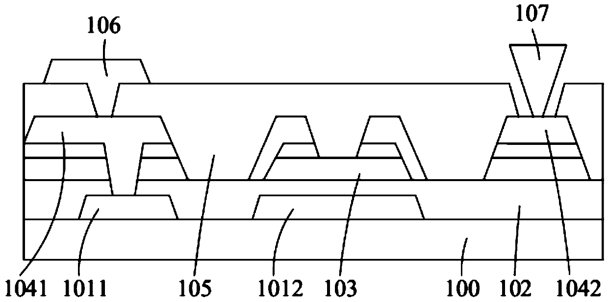
Figure 1 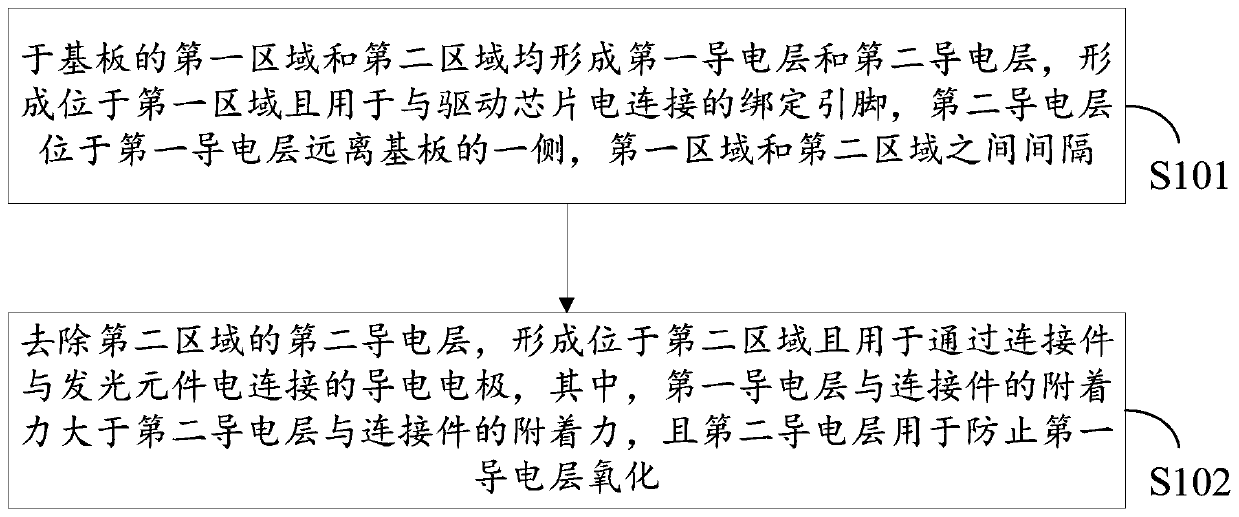
Figure 2 
Figure 3
Abstract
Description
technical field
[0001] The present application relates to the field of display technology, in particular to an array substrate, a manufacturing method thereof, and a display device. Background technique
[0002] Such as figure 1 As shown in FIG. 2 , it is a schematic diagram of a conventional submillimeter light emitting diode (Mini Light Emitting Diode, Mini-LED) backlight module. The traditional submillimeter light-emitting diode backlight module includes: a first metal pattern layer formed on the substrate 100, the first metal pattern layer includes a first conductive member 1011 and a gate 1012; the gate covering the first metal pattern layer and the substrate 100 The insulating layer 102; the active layer 103 formed on the gate insulating layer 102; the second metal pattern layer formed on the side of the active layer 103 away from the substrate 100, the second metal pattern layer includes a second conductive member 1041, a source-drain circuit Pole and conductive ele...
Examples
Embodiment Construction
[0034] The technical solutions in the embodiments of the present application will be clearly and completely described below in conjunction with the drawings in the embodiments of the present application. Apparently, the described embodiments are only some of the embodiments of this application, not all of them. Based on the embodiments in this application, all other embodiments obtained by those skilled in the art without making creative efforts belong to the scope of protection of this application.
[0035] see figure 2 , which is a flowchart of a method for manufacturing an array substrate according to an embodiment of the present application. The manufacturing method of the array substrate includes the following steps:
[0036] S101: Form a first conductive layer and a second conductive layer on both the first area and the second area of the substrate, form a binding pin located in the first area and used for electrical connection with the driver chip, and the second c...