
Passivation encapsulation method for organic electro luminescence elements and structure
A packaging structure and packaging method technology, applied to electrical components, lighting devices, light sources, etc., can solve the problems of high cost, high equipment cost, poor barrier layer coverage, high production cost, etc., to improve the step effect, simplify the manufacturing process, improve The effect of production efficiency
Patent Information
- Authority / Receiving Office
- CN · China
- Current Assignee / Owner
- Publication Date
- 2004-08-11
- Estimated Expiration
- Not applicable · inactive patent
Smart Images
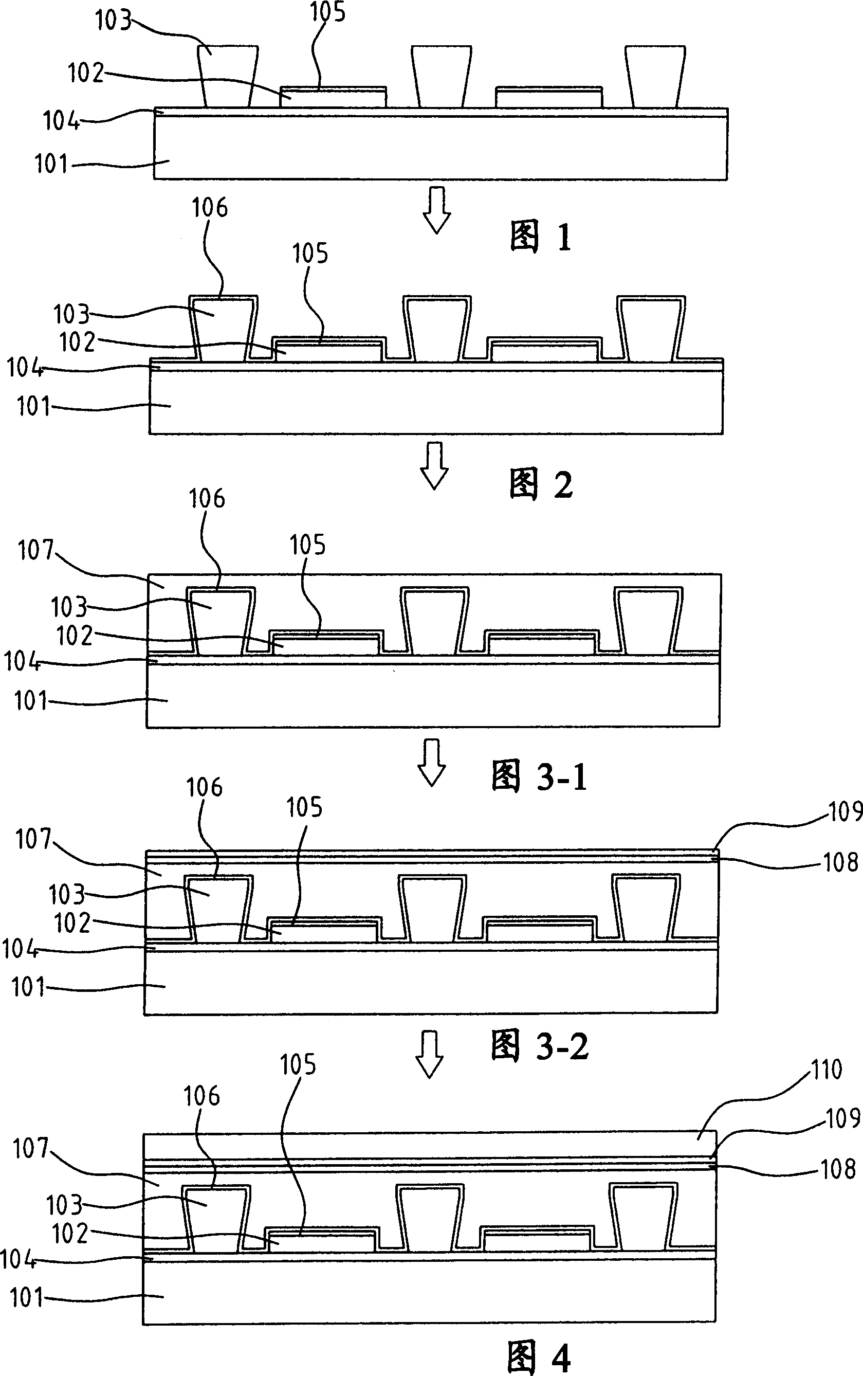
Figure 1 
Figure 2 
Figure 3
Abstract
Description
technical field
[0001] The present invention relates to a polymer layer coated by spraying or screen printing developed to ensure that the interior of the element is not affected by the external environment in an organic light-emitting diode (OLED) element, so as to protect the substrate formed on the substrate. The encapsulation method and structure of the organic electroluminescent (EL) element. Background technique
[0002] Organic EL elements are elements with a layered structure, and the materials of each layer are extremely sensitive to the external environment. In order to facilitate the injection of electrons, the cathode uses a material with a low work function, but the material with a low work function is easily oxidized, and the oxidation of the cathode material will greatly reduce the efficiency of the element. In addition, the light-emitting layer formed by fluorescent organic solids of the device and the injection layer and transport layer of electrons and hol...
Examples
Embodiment Construction
[0026] As shown in Fig. 1~Fig. 4, be embodiment of the present invention, show a kind of barrier (passivation) encapsulation method of organic EL element, this method comprises the following steps:
[0027] As shown in Figure 1, for the step of providing a transparent substrate 101, a plurality of organic EL element pixels 102 have been formed on the transparent substrate 101, and have a plurality of ribs (rib) 103; There is an ITO anode layer 104 as the anode of the organic EL element pixel 102, and the organic EL element pixel 102 has a cathode layer 105 on the upper surface, and the purpose of designing the ribs 103 is to prevent the cross talk phenomenon of the element.
[0028] As shown in Figure 2, for the step of forming a protective layer, a cathodic protective layer 106 is plated on the surface of the organic EL element pixel 102, which is an inorganic material layer; and the protective layer 106 is formed by a low-temperature chemical vapor deposition method Formed b...