
Active semiconductor nuclear radiation detector for converting nuclear radiation into luminescence
A semiconductor and N-type semiconductor technology, applied in the field of nuclear radiation detection, can solve the problems of slow decay time, low luminous efficiency, difficult to control, etc., and achieve the effect of improving the overall efficiency, high luminous efficiency, and high-efficiency conversion
Patent Information
- Authority / Receiving Office
- CN · China
- Current Assignee / Owner
- Publication Date
- 2022-01-18
Smart Images
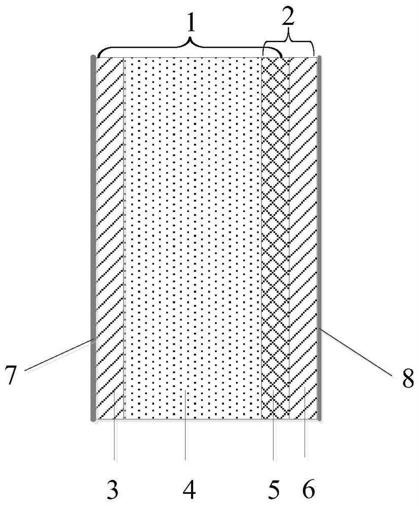
Figure 1 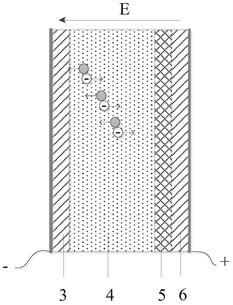
Figure 2 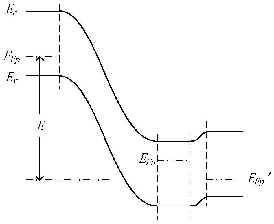
Figure 3
Abstract
Description
technical field
[0001] The invention belongs to nuclear radiation detection technology, and relates to an active semiconductor nuclear radiation detection device that converts nuclear radiation into luminescence, which can replace the function of a traditional scintillator. Background technique
[0002] Scintillator is a very important basic material for nuclear radiation detection. Its function is to convert high-energy particles and rays into light. The detection of high-energy particles and rays can be realized by measuring the luminescence of scintillators. It is used in high-energy physics and nuclear physics experiments, It is widely used in nuclear medical imaging, environmental monitoring gamma energy spectroscopy and other fields, and it is also an indispensable key material for neutrons in pulsed radiation fields, gamma diagnosis and construction of pulsed radiation imaging systems. Luminescence efficiency and luminescence time are two important parameters of scint...
Examples
Embodiment Construction
[0029] Now in conjunction with embodiment, accompanying drawing, the present invention will be further described:
[0030] The electro-optic coupling nuclear radiation detection device of the embodiment of the present invention has a main body structure of a flat plate, which is composed of a PIN structure 1 and an LED light-emitting diode 2 connected in series, both of which share an N layer or a P layer. It is characterized in that, if the N layer is shared, the PIN structure 1 is composed of P-type semiconductor material 3, intrinsic semiconductor material 4 and N-type semiconductor material 5; the LED light-emitting diode 2 is composed of N-type semiconductor material 5 and P-type semiconductor material Material 6 composition. Multiple layers of different types of semiconductor materials are stacked to form a PINP structure, and electrodes 7 and 8 are respectively fabricated on the surface of the device.
[0031] The PIN structure 1 and the LED light-emitting diode 2 are ...