
Power converter module
a power converter module and module technology, applied in the direction of cross-talk/noise/interference reduction, inductance with magnetic core, inductance, etc., can solve the problems of increasing the proportion of this loss in the total loss of the power converter module, reducing and increasing the ac loss. , to achieve the effect of reducing the parasitic loss, and improving the conversion efficiency of the power conversion modul
Patent Information
- Authority / Receiving Office
- US · United States
- Patent Type
- Patents(United States)
- Current Assignee / Owner
- Publication Date
- 2022-02-15
Smart Images
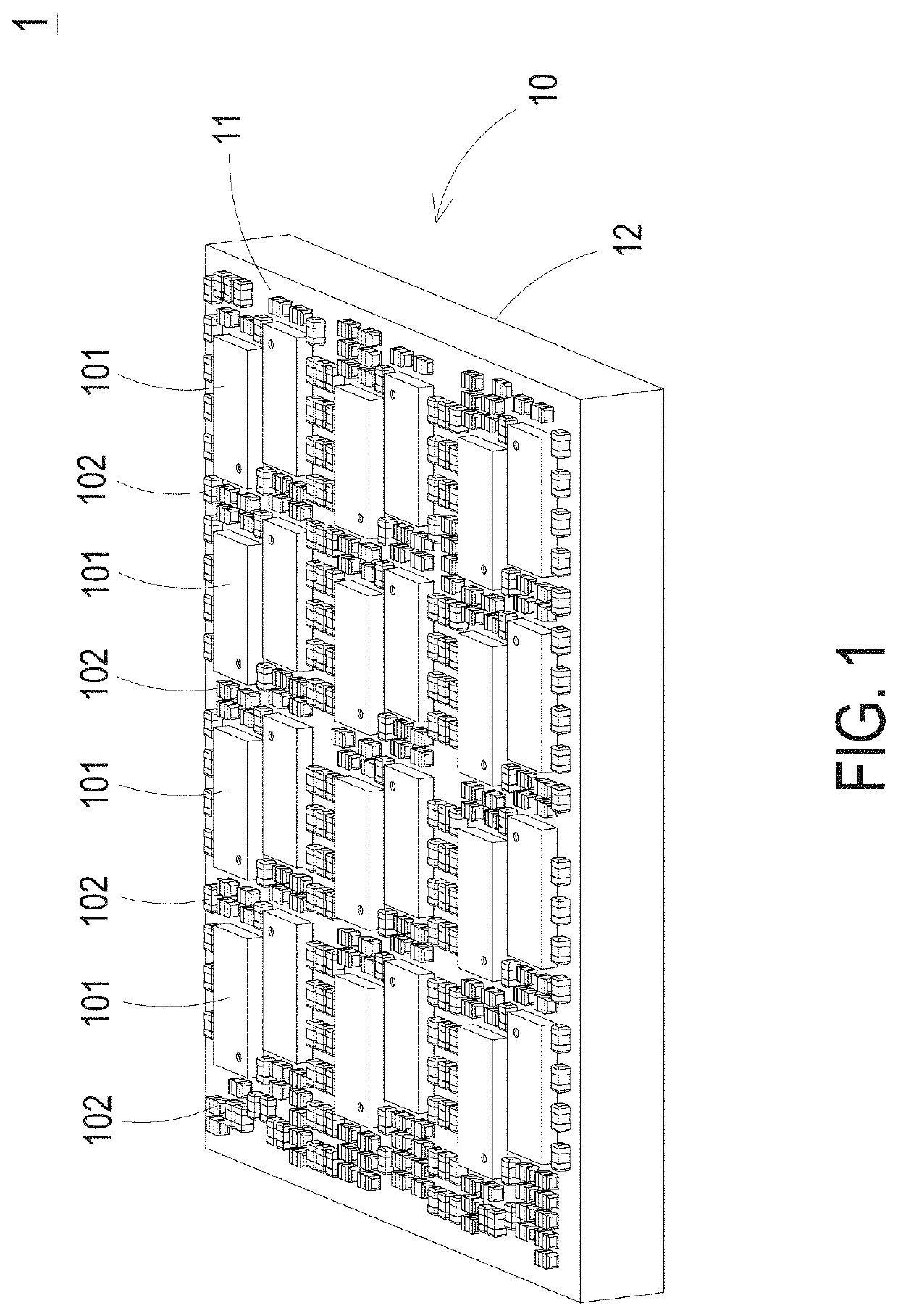
Figure 1 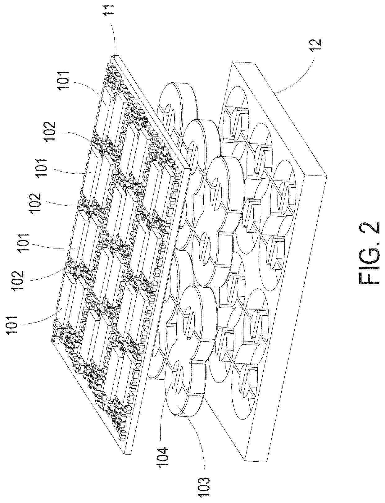
Figure 2 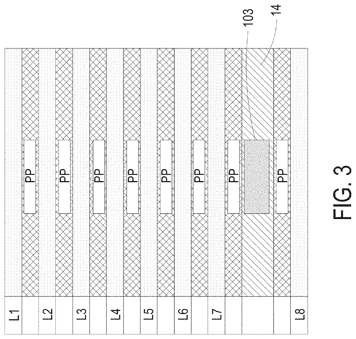
Figure 3
Abstract
Description
CROSS-REFERENCE TO RELATED APPLICATION
[0001] This application claims priorities to China Patent Application No. 202011164463.3 filed on Oct. 27, 2020, and China Patent Application No. 202011239669.8 filed on Nov. 9, 2020, the entire content of which is incorporated herein by reference for all purposes.FIELD OF THE INVENTION
[0002] The present disclosure relates to a power converter module, and more particularly to a power converter module with a plurality of positive copper layers and a plurality of negative copper layers staggered.BACKGROUND OF THE INVENTION
[0003] With the rapid development of technologies such as mobile communications and cloud computing, high-power power converter modules have been widely used in electronic products. Due to the trend of high power and miniaturization of electronic products, how to improve the conversion efficiency of the power converter module and reduce the size of the power converter module is the primary consideration.
[0004] As the output power of ...
Examples
Embodiment Construction
[0016]The present disclosure will now be described more specifically with reference to the following embodiments. It is to be noted that the following descriptions of preferred embodiments of this disclosure are presented herein for purpose of illustration and description only. It is not intended to be exhaustive or to be limited to the precise form disclosed.
[0017]FIG. 1 is a schematic perspective view illustrating a power converter module according to an embodiment of the present disclosure. FIG. 2 is an exploded view illustrating the power converter module according to the embodiment of the present disclosure. FIG. 3 is a schematic side view illustrating the power converter module according to the embodiment of the present disclosure. FIG. 4 is a schematic side view illustrating the power converter module according to the embodiment of the present disclosure. As shown in FIGS. 1, 2, 3, and 4, the power converter module 1 includes a multilayer printed circuit board 10, at least on...