
Optical modulator
a modulator and optical technology, applied in the field of optical modulators, can solve the problems of limiting the length of high-speed modulation, and the entire length of the modulator is as long as about 10 cm, and achieve the effect of reducing dc drift and stabilizing the structure over a long period of tim
Patent Information
- Authority / Receiving Office
- US · United States
- Patent Type
- Patents(United States)
- Current Assignee / Owner
- Publication Date
- 2022-06-21
Smart Images
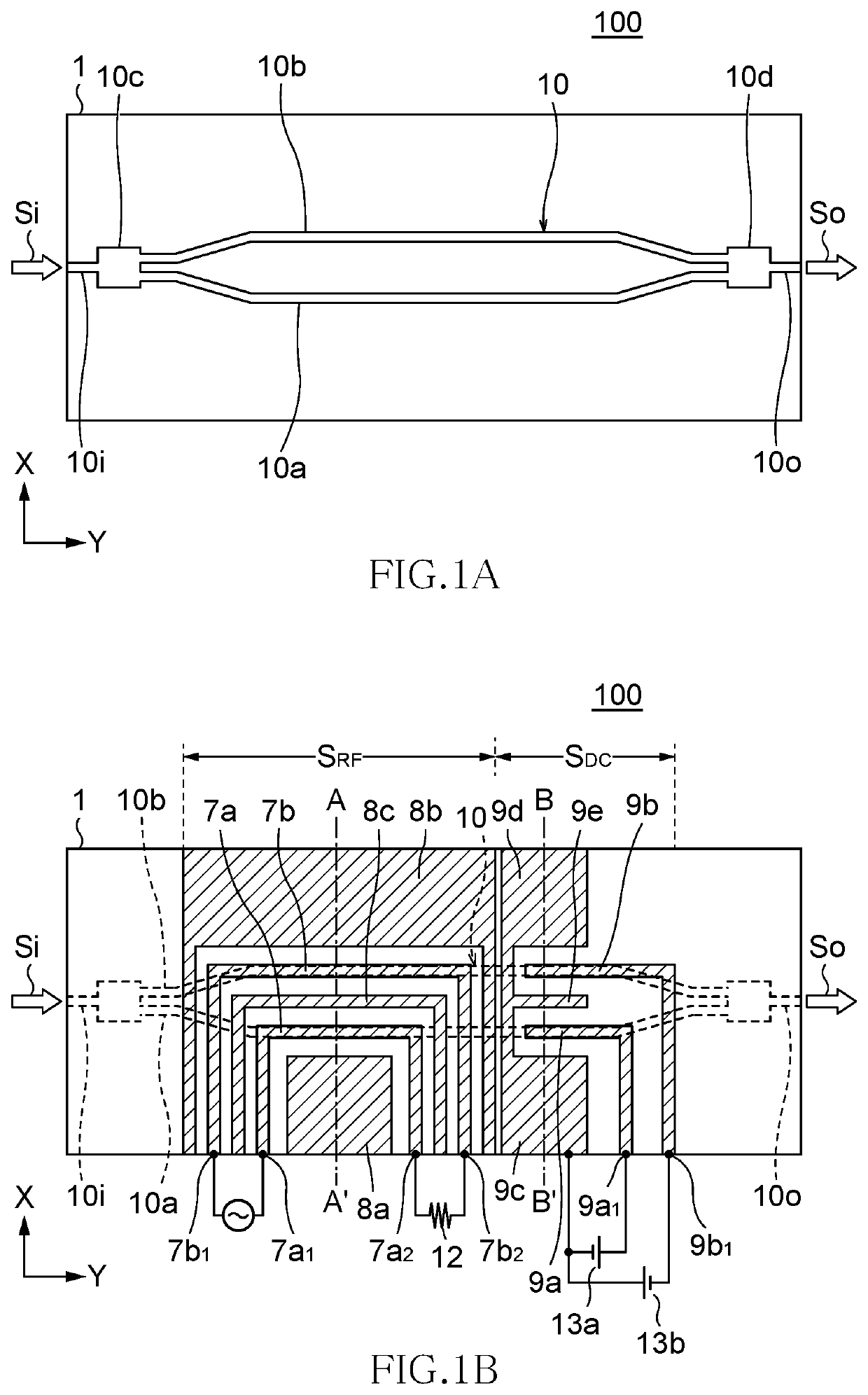
Figure 1 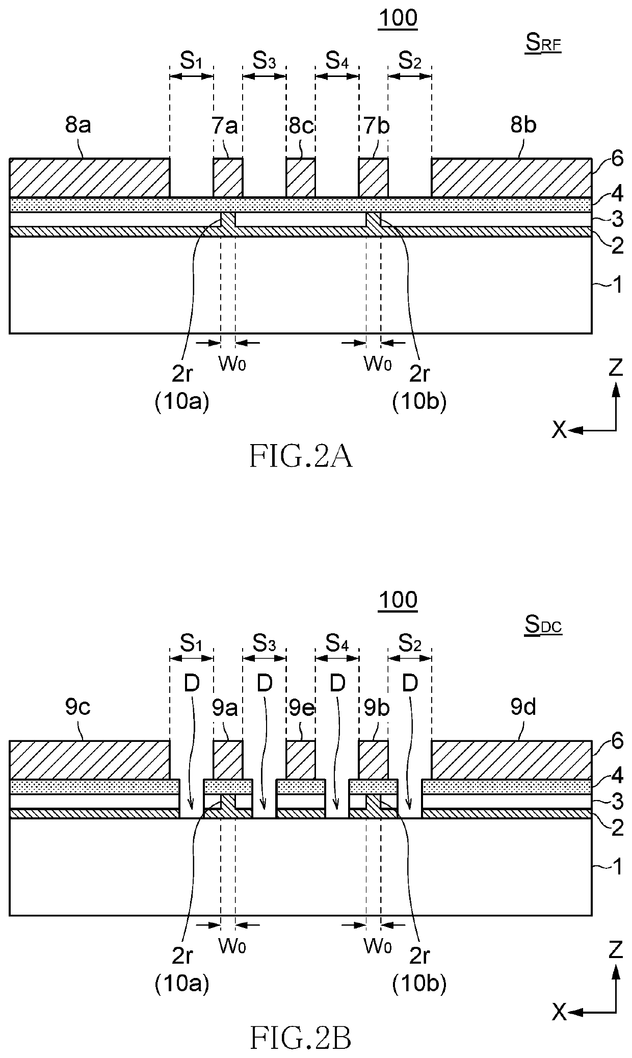
Figure 2 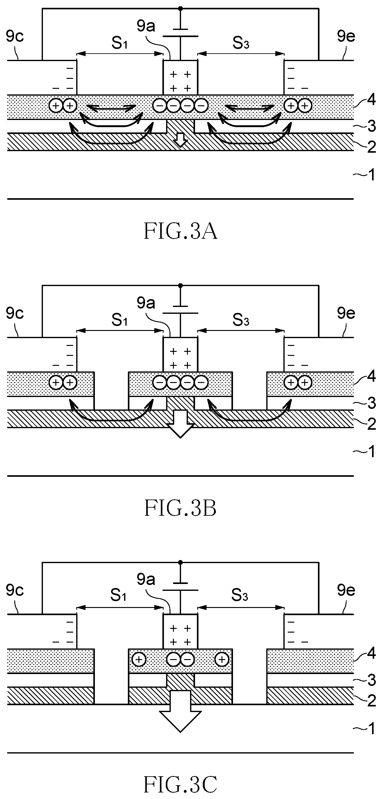
Figure 3
Abstract
Description
CROSS REFERENCE TO RELATED APPLICATIONS
[0001] This application is the U.S. National Phase under 35 U.S.C. § 371 of International Application No. PCT / JP2018 / 036329, filed on Sep. 28, 2018, which claims the benefit of Japanese Patent Application No. 2017-192812, filed on Oct. 2, 2017, the entire contents of each are hereby incorporated by reference.TECHNICAL FIELD
[0002] The present invention relates to an optical modulator used in the fields of optical communication and optical measurement and, more particularly, to an electrode structure of a Mach-Zehnder optical modulator.BACKGROUND ART
[0003] Communication traffic has been remarkably increased with widespread Internet use, and optical fiber communication is becoming significantly important. The optical fiber communication is a technology that converts an electric signal into an optical signal and transmits the optical signal through an optical fiber and has wide bandwidth, low loss, and resistance to noise.
[0004] As a system for convert...
Examples
examples
[0118]An acceleration test as to the DC drift was carried out for the optical modulators according to Comparative Examples and Examples. In this acceleration test, a change in drift amount Vdrift / Vbias when a DC bias Vbias was continued to be applied for 24 hours under a high temperature of 140° C. was determined.
[0119]Optical modulators according to Comparative Examples 1A and 1B each have the cross-sectional structure of FIG. 3A, that is, they each have a conventional structure in which the waveguide layer and buffer layer are formed over the entire surface. The buffer layer of Comparative Example 1A is formed of an oxide La—Al—O (composition A) containing La and Al as main components, and the buffer layer of Comparative Example 1B is formed of an oxide Si—In—O (composition B) containing Si and In as main components.
[0120]Optical modulators according to Comparative Examples 2A and 2B each have the cross-sectional structure of FIG. 3B, that is, they each have a conventional structu...