
High density nanostructured interconnection
a nano-structured, high-density technology, applied in the direction of vehicle sub-unit features, instrumentation, semiconductor/solid-state device details, etc., can solve the problems of increasing the risk of damage to the increasingly fragile components, damage to the mems package, damage to the mems components,
Patent Information
- Authority / Receiving Office
- US · United States
- Patent Type
- Applications(United States)
- Current Assignee / Owner
- Publication Date
- 2005-10-13
Smart Images
Figure 1 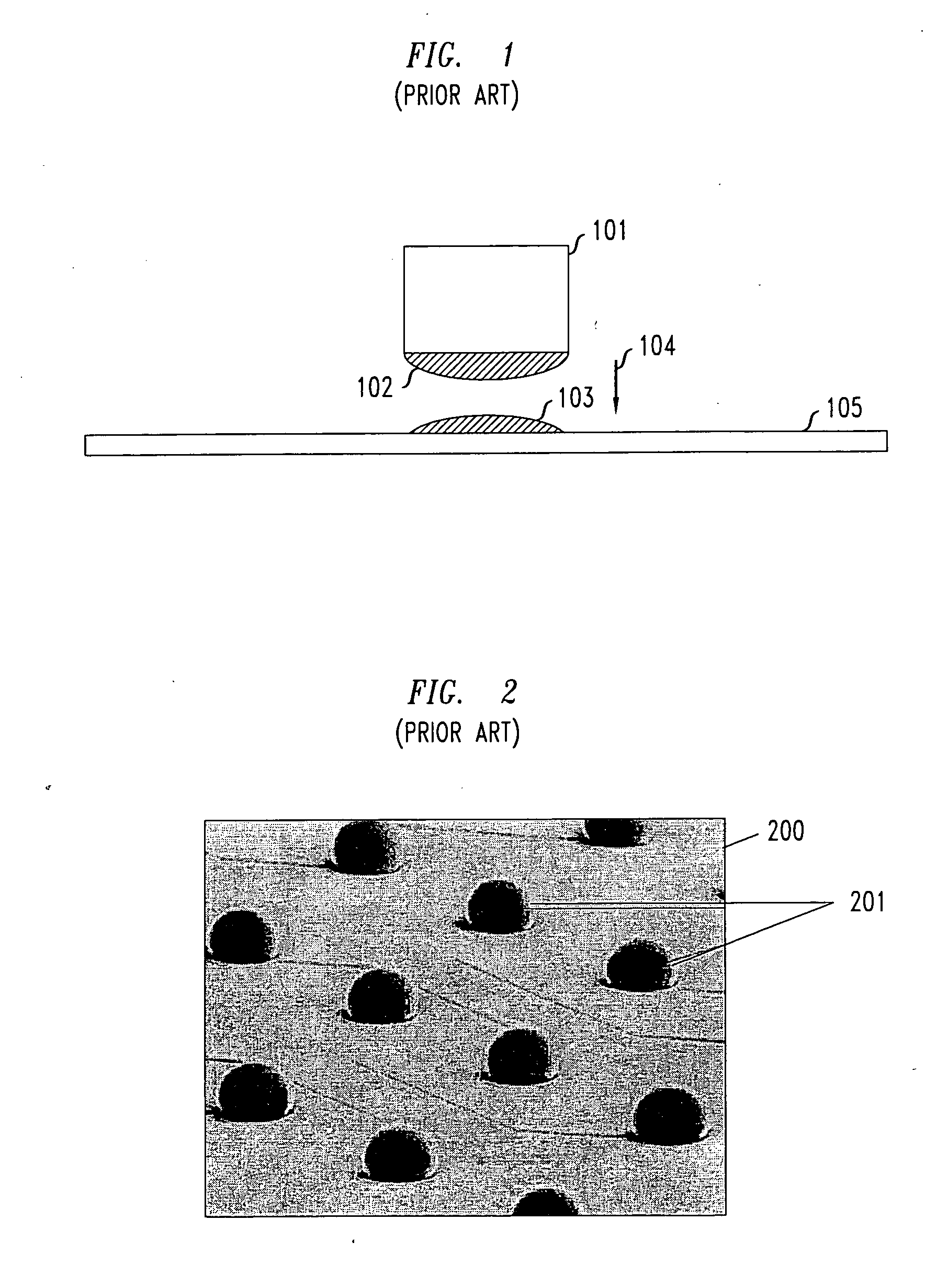
Figure 2 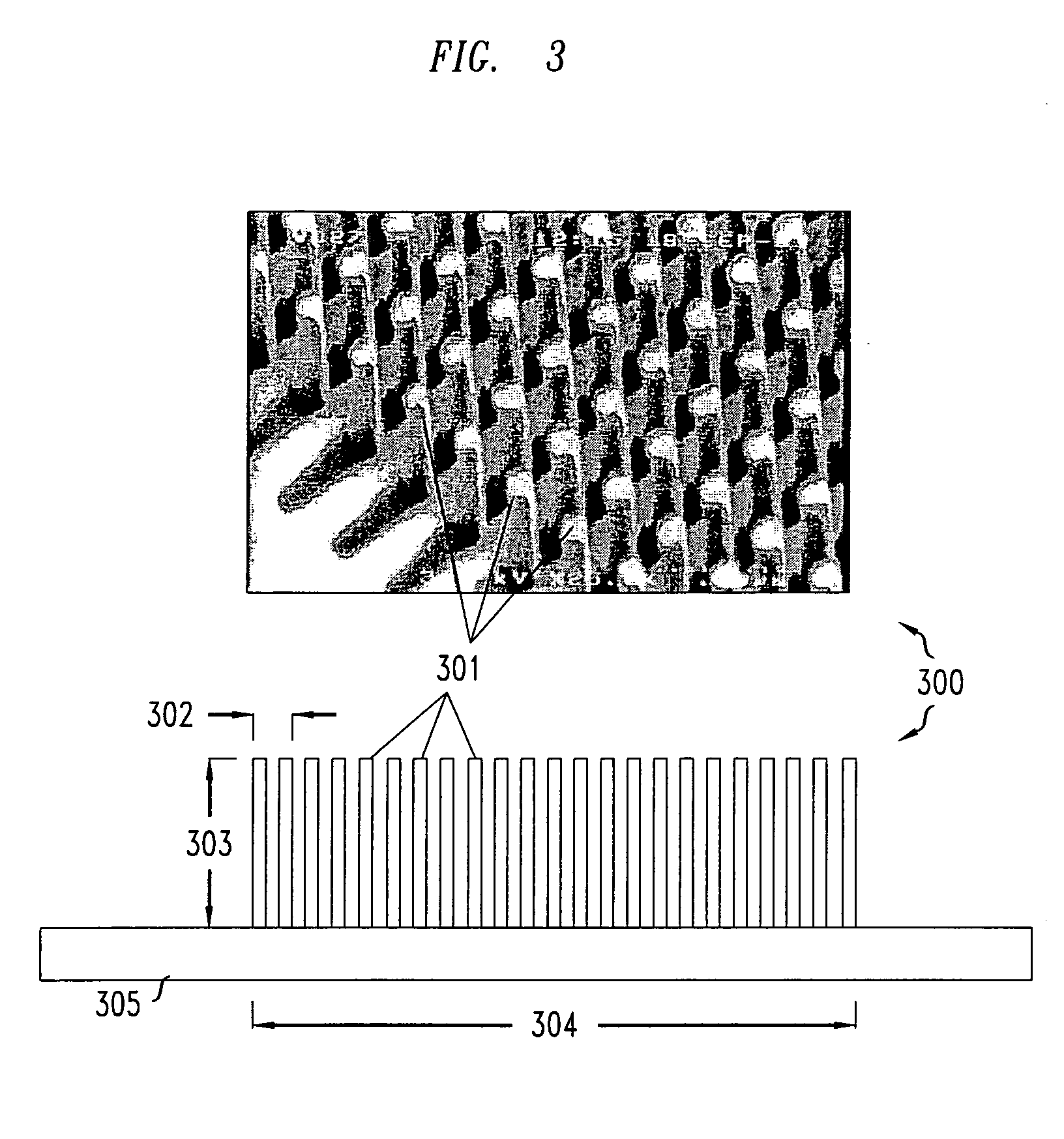
Figure 3
Abstract
Description
FIELD OF THE INVENTION
[0001] The present invention relates generally to thermal and electrical interconnections and, more particularly, to nanostructured thermal and electrical interconnections. BACKGROUND OF THE INVENTION
[0002] Methods for electrically or thermally connecting electronics components onto, for example, a conductor or semiconductor substrate are well known in the art. For example, both thermo-compression and solder bump bonding methods have been used to create connections between, illustratively, components in optoelectronic devices and / or microelectromechanical (MEMS) devices. FIG. 1 shows one illustrative method of forming a thermo-compression bond for use as a thermal or electrical interconnection. Specifically, in that figure, component 101 has a layer of a material 102, typically gold, which is suitable for compression bonding. In order to bond component 101 with illustrative substrate 105, layer 102 on component 101 is, for example, lowered in direction 104 in...
Examples
Embodiment Construction
[0014]FIG. 3 shows one illustrative surface 300 in accordance with the principles of the present invention whereby a plurality of nanostructures 301, here nanoposts, are manufactured on a substrate 305, such as a silicon substrate. Cylindrical nanopost arrays, such as that shown in FIG. 3, have been produced with each nanopost having a diameter of less than 10 nm. One skilled in the art will recognize that there are many different illustrative arrangements (e.g., sizes, pitch and height) of nanoposts that can be produced using various methods and that such various diameter nanoposts can be fashioned with different degrees of regularity. An illustrative method of producing nanoposts, found in U.S. Pat. No. 6,185,961, titled “Nanopost arrays and process for making same,” issued Feb. 13, 2001 to Tonucci, et al, is hereby incorporated by reference herein in its entirety. Nanoposts have been manufactured by various methods, such as by using a template to form the posts, by various means ...