
Dummy Phase Shapes To Reduce Sensitivity Of Critical Gates To Regions Of High Pattern Density
Patent Information
- Authority / Receiving Office
- US · United States
- Current Assignee / Owner
- Publication Date
- 2007-12-06
- Estimated Expiration
- Not applicable · inactive patent
Smart Images
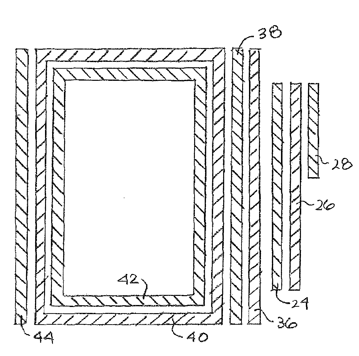
Figure 1 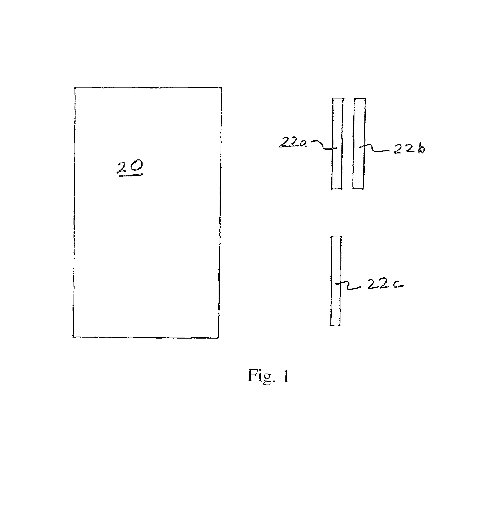
Figure 2 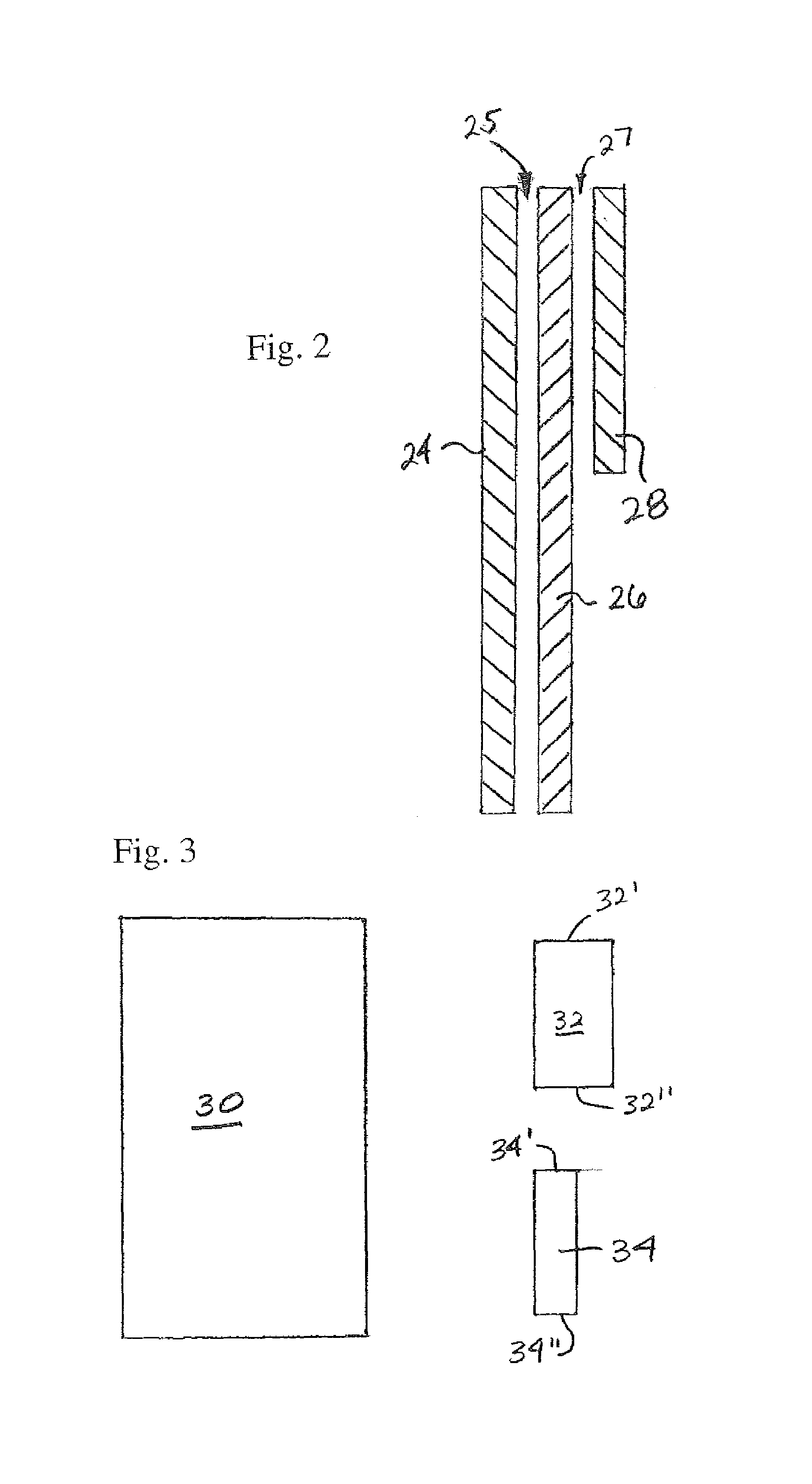
Figure 3
Abstract
Description
BACKGROUND OF THE INVENTION
[0001] 1. Field of the Invention
[0002] The present invention is directed to the manufacture of masks used in the lithographic production of integrated circuits and, in particular, to the manufacture of alternating phase shifting masks.
[0003] 2. Description of Related Art
[0004] Polysilicon gate dimensional control is of critical importance for advanced semiconductor technologies. Two-mask alternating phase shift lithography offers improved resolution and dimensional control relative to competing one-mask solutions such as attenuated phase shift lithography. With alternating phase shift mask (altPSM) processing, a first phase mask is used to image the small, features in a design of critical dimension. As used herein, the term critical dimension refers to any dimension smaller than the smallest dimension that can be printed within a specified tolerance by a lithographic process without the need for a resolution enhancement technique such as alternating phase shi...
Examples
Embodiment Construction
)
[0020]In describing the preferred embodiment of the present invention, reference will be made herein to FIGS. 1-5 of the drawings in which like numerals refer to like features of the invention.
[0021]The method of designing an alternating phase shifting mask of the present invention is most useful in connection with integrated circuit design features employed in semiconductor applications in which the linewidth sensitive feature is in the gate region of a transistor. In FIG. 1, there is depicted an exemplary portion of an integrated circuit layout design comprising segments that includes a large polysilicon feature 20 such as a decoupling capacitor, and adjacent narrow polysilicon gate structures 22a, 22b, 22c, for which dimensional control is of critical importance. These gate structures of the integrated circuit design have a critical width along their lengths, and are all parallel.
[0022]When these features are projected onto a wafer resist layer by a conventional two mask lithogr...