
RF integrated circuit with ESD protection and ESD protection apparatus thereof
a protection apparatus and integrated circuit technology, applied in electrical devices, semiconductor devices, semiconductor/solid-state device details, etc., can solve the problems of damage to semiconductor devices, inability to avoid the impact of electrostatic discharge, and damage to parts of devices, so as to achieve the effect of reducing fabrication costs and substantially saving chip area
Patent Information
- Authority / Receiving Office
- US · United States
- Current Assignee / Owner
- Publication Date
- 2007-12-27
- Estimated Expiration
- Not applicable · inactive patent
Smart Images
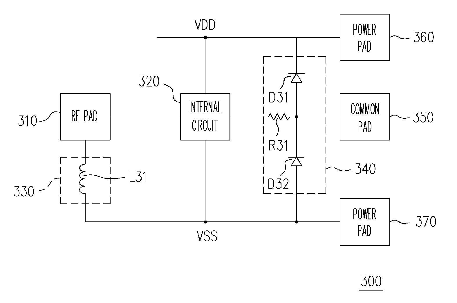
Figure 1 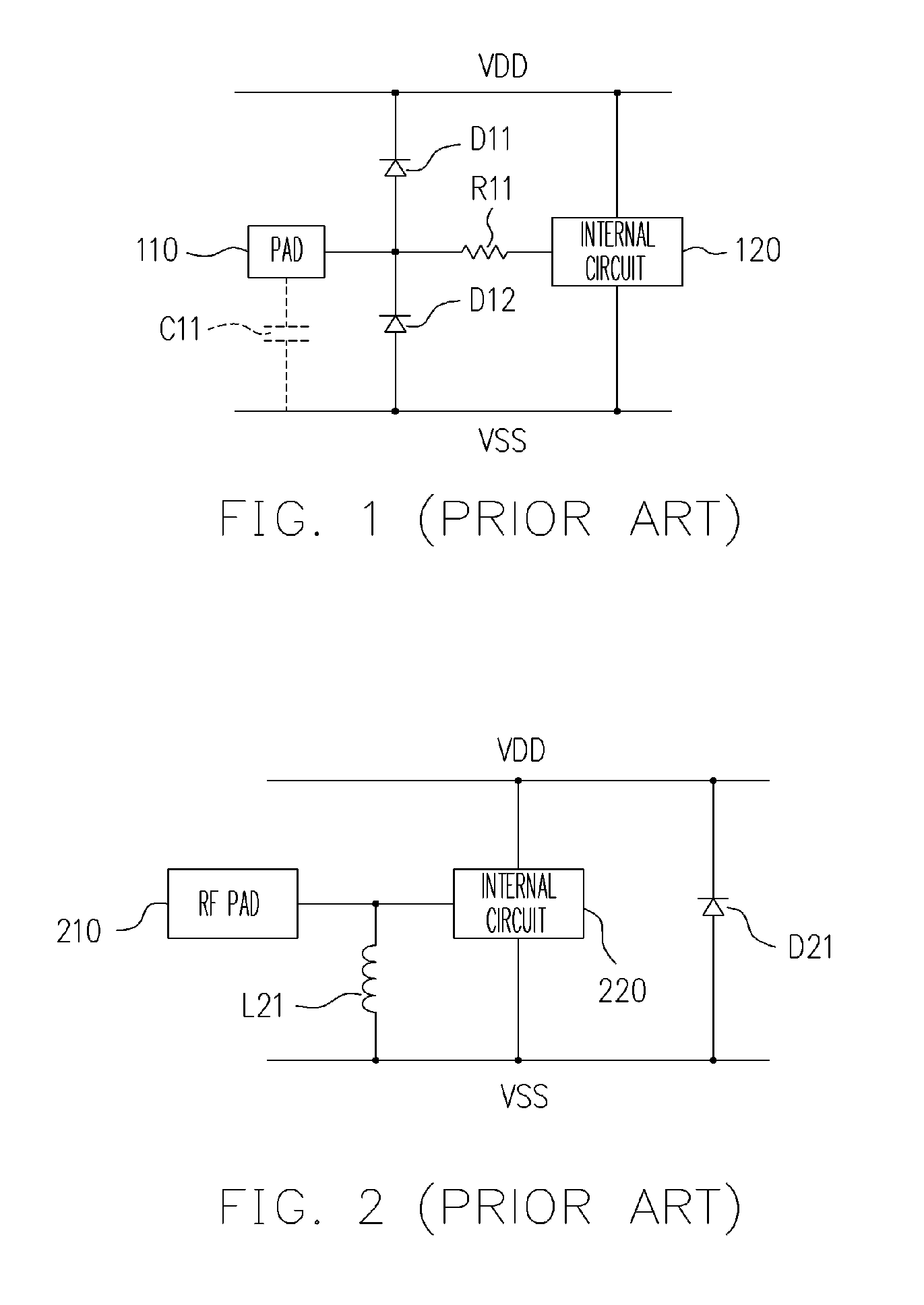
Figure 2 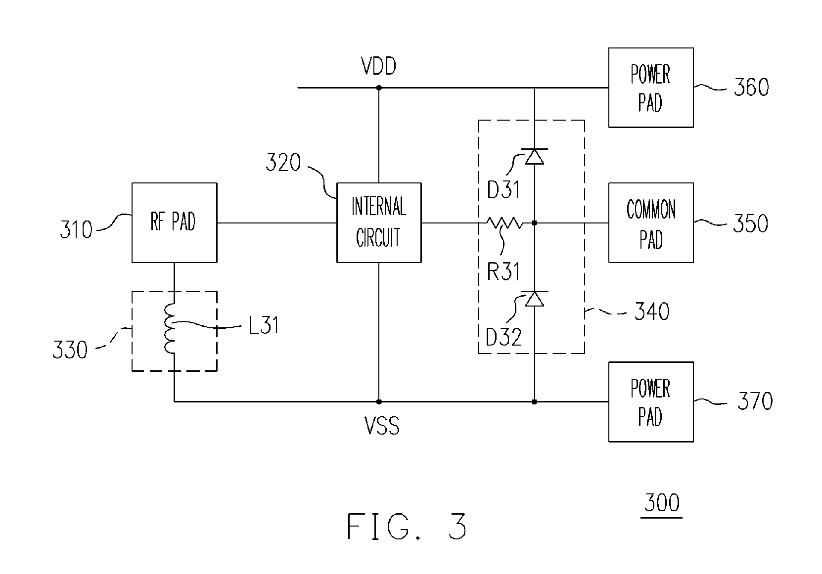
Figure 3
Abstract
Description
BACKGROUND OF THE INVENTION
[0001] 1. Field of Invention
[0002] The present invention relates to an electrostatic discharge (ESD) protection apparatus. More particularly, the present invention relates to a radio frequency (RF) integrated circuit with ESD protection and an ESD protection apparatus thereof.
[0003] 2. Description of Related Art
[0004] Electrostatic discharge can be substantially divided into human-body model (HBM), machine model (MM), and charge-device model (CDM). The electrostatic discharge impact can not be avoided in the electronic circuit in actual usage environment, and part of the devices may be damaged if there is no suitable protection means. When an electrostatic discharge occurs, a great deal of electrostatic discharge current may produce high temperature that may damage the semiconductor devices. Therefore, how to protect the internal circuit of the integrated circuit from the impact of the electrostatic discharge current is crucial. In order to avoid the abovement...
Examples
Embodiment Construction
[0025]FIG. 3 is a block diagram of an RF integrated circuit with ESD protection according to the embodiment of the present invention. Please referring to FIG. 3, in the RF integrated circuit 300, an internal circuit 320 receives / emits an RF signal and a common signal respectively through an RF bonding pad 310 and a common bonding pad 350. The power for the internal circuit 320 is provided from outside through a power rail VDD, a power bonding pad 360, a power rail VSS, and a power bonding pad 370. In the embodiment, the power rail VDD is a system voltage rail, and the power rail VSS is a ground rail. In the normal operation, the power rails VSS and VDD are suitable to respectively provide a ground voltage and a system voltage to the internal circuit 120. It needs to be noted that FIG. 3 is a simplified embodiment, and the quantity of actual various pads is not limited by the number shown in FIG. 3.
[0026]Usually, a group of ESD protection circuits (for example, ESD protection circuit...