
Printed circuit board having stepped conduction layer
a technology of conduction layer and printed circuit board, which is applied in the direction of printed circuit aspects, high frequency circuit adaptations, cross-talk/noise/interference reduction, etc., can solve the problems of reducing the efficiency of the circuit board, increasing the complexity of the electronic device, and using a decoupling capacitor, so as to reduce the manufacturing time and manufacture costs
Patent Information
- Authority / Receiving Office
- US · United States
- Patent Type
- Applications(United States)
- Current Assignee / Owner
- Publication Date
- 2009-04-02
- Estimated Expiration
- Not applicable · inactive patent
Smart Images
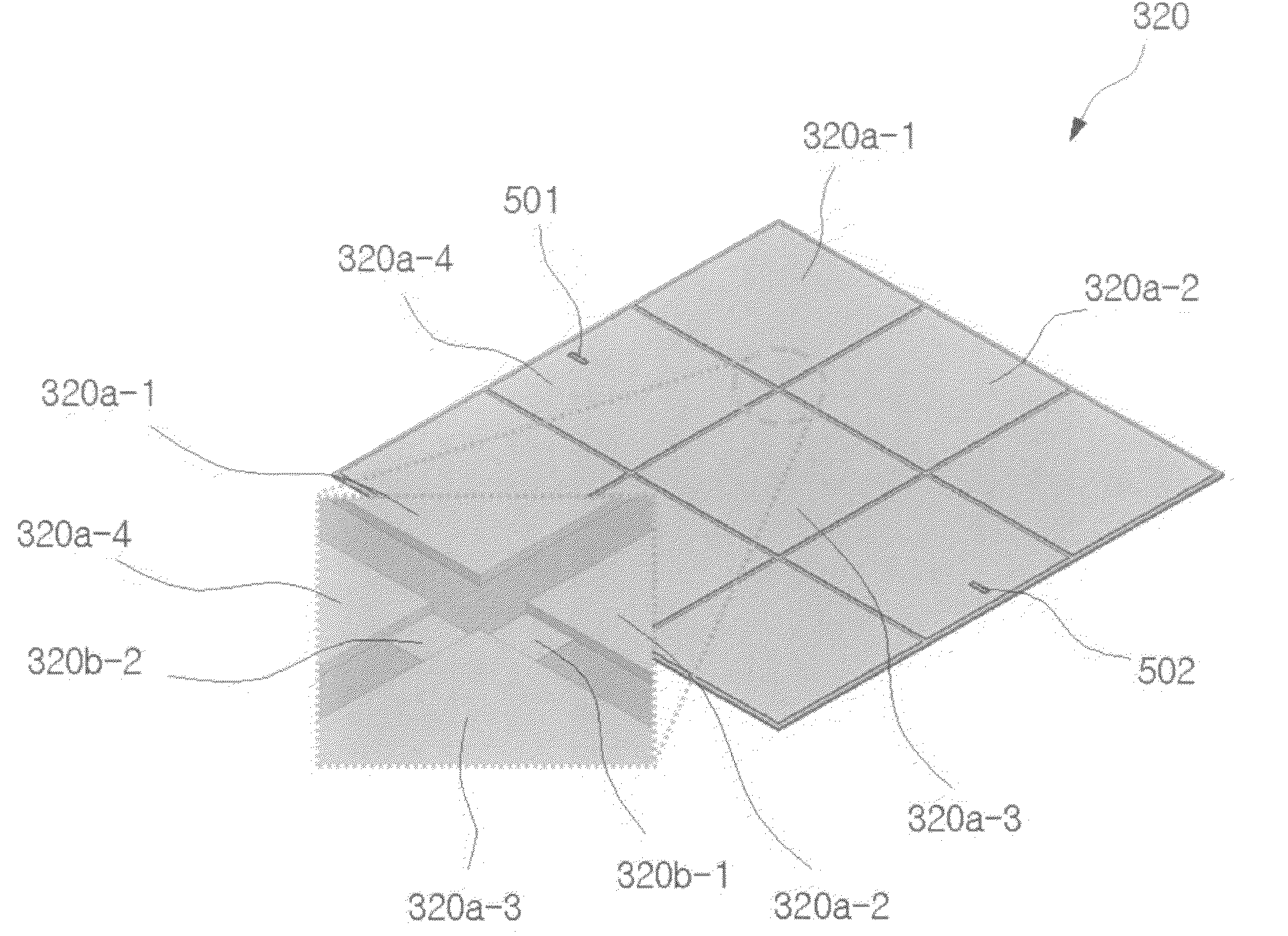
Figure 1 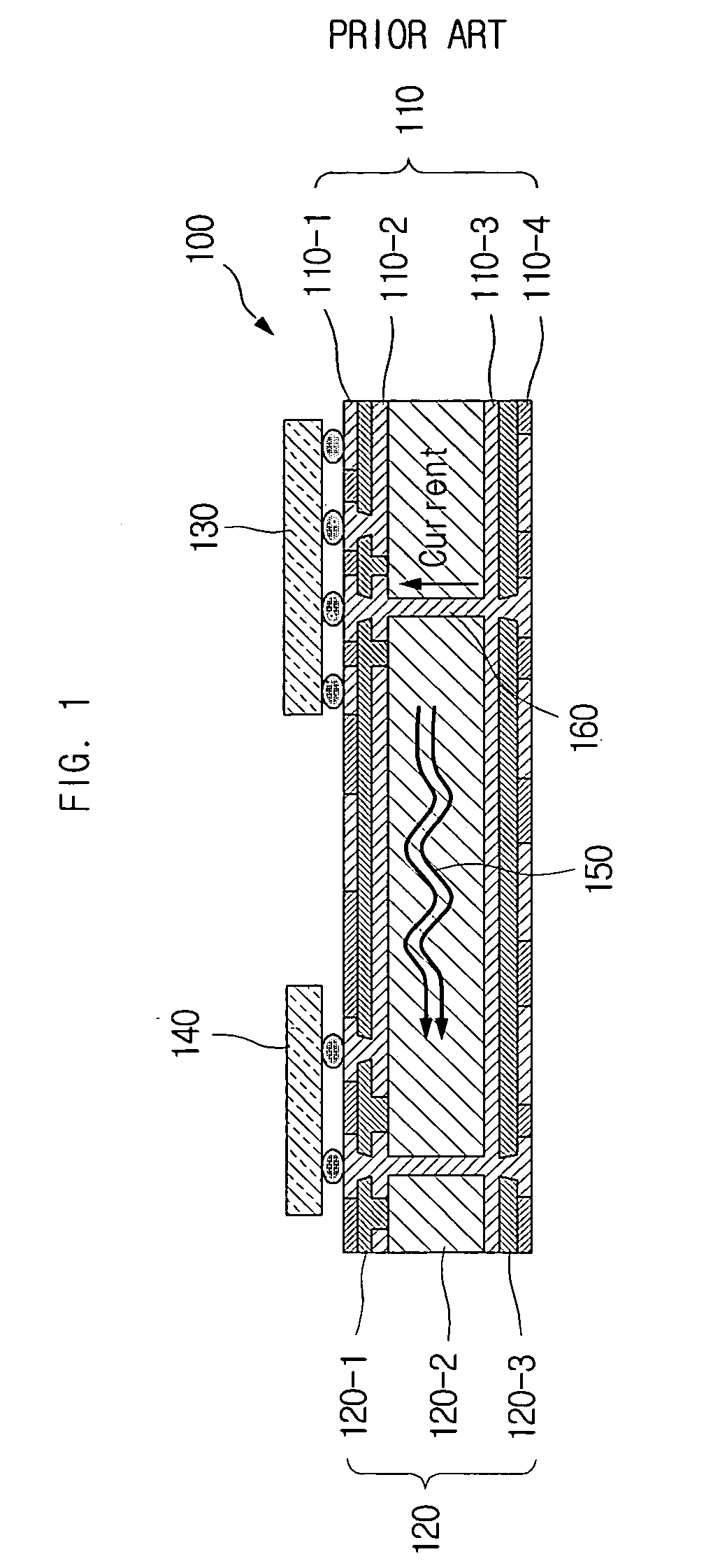
Figure 2 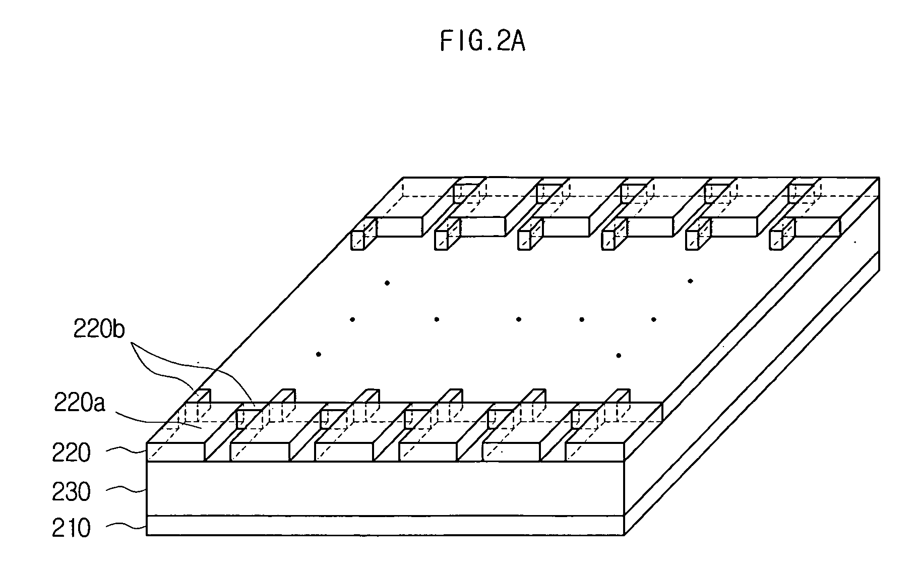
Figure 3
Abstract
Description
CROSS-REFERENCE TO RELATED APPLICATIONS
[0001] This application claims the benefit of Korean Patent Application No. 10-2007-0097721 filed with the Korean Intellectual Property Office on Sep. 28, 2007, the disclosure of which is incorporated herein by reference in its entirety.BACKGROUND
[0002] 1. Technical Field
[0003] The present invention relates to a printed circuit board, more particularly to a printed circuit board having a stepped conduction layer.
[0004] 2. Description of the Related Art
[0005] Portability has become a critical feature of current electronic devices, and various devices allowing wireless communication have appeared in the market, such as mobile communication terminals, PDA's (personal digital assistants), laptops, DMB (digital multimedia broadcasting) equipment, etc.
[0006] To enable wireless communication, such devices generally include printed circuit boards that have both analog circuits (for example, an RF circuit) and digital circuits.
[0007] FIG. 1 is a cross-sectiona...
Examples
Embodiment Construction
[0051]As the present invention allows for various changes and numerous embodiments, particular embodiments will be illustrated in drawings and described in detail in the written description. However, this is not intended to limit the present invention to particular modes of practice, and it is to be appreciated that all changes, equivalents, and substitutes that do not depart from the spirit and technical scope of the present invention are encompassed in the present invention. In the description of the present invention, certain detailed explanations of related art are omitted when it is deemed that they may unnecessarily obscure the essence of the invention.
[0052]While such terms as “first” and “second,” etc., may be used to describe various elements, such elements must not be limited to the above terms. The above terms are used only to distinguish one element from another. For example, a first element may be referred to as a second element without departing from the scope of right...