
Interconnect manufacturing process
Patent Information
- Authority / Receiving Office
- US · United States
- Current Assignee / Owner
- Publication Date
- 2009-04-02
- Estimated Expiration
- Not applicable · inactive patent
Smart Images
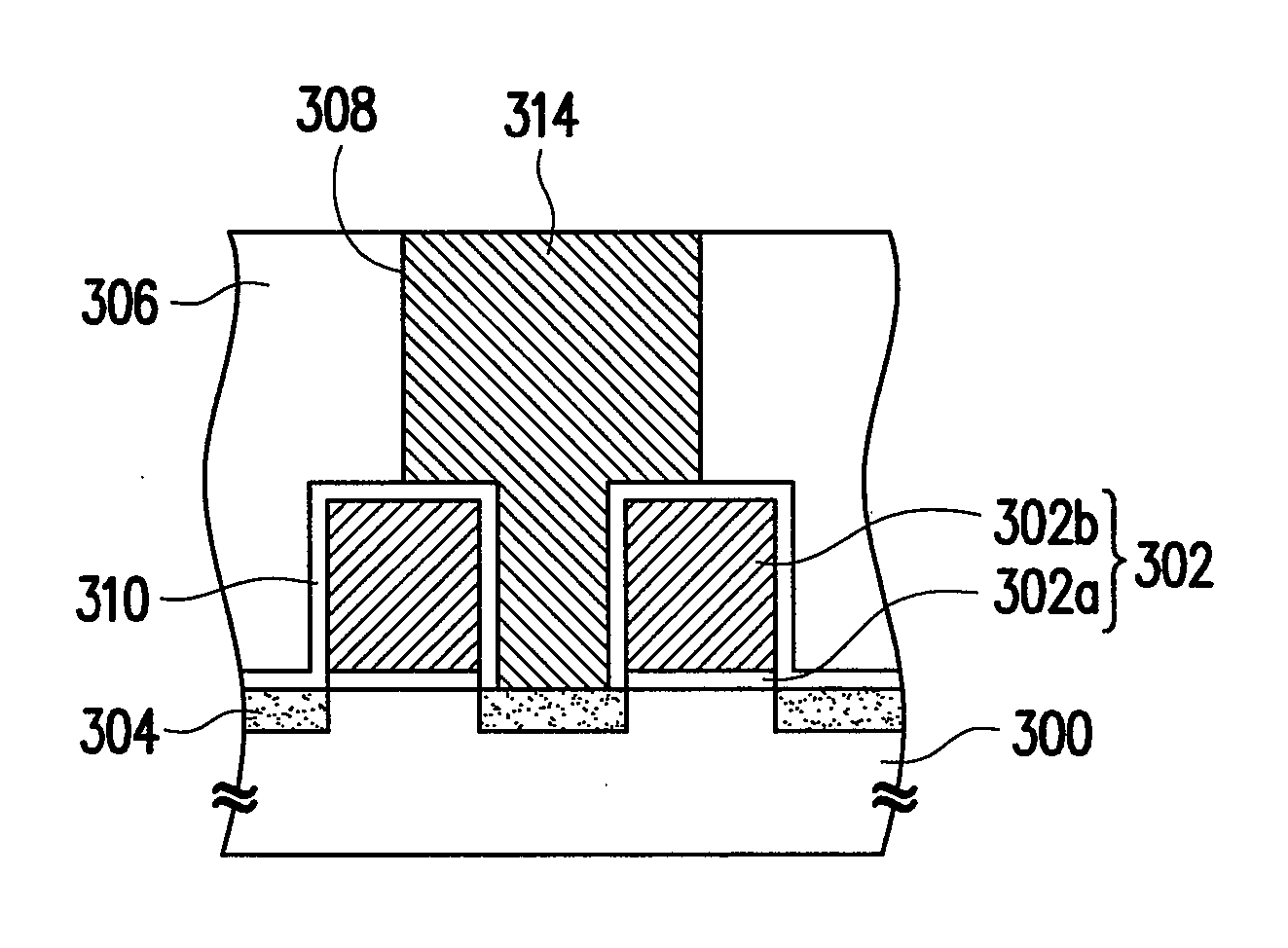
Figure 1 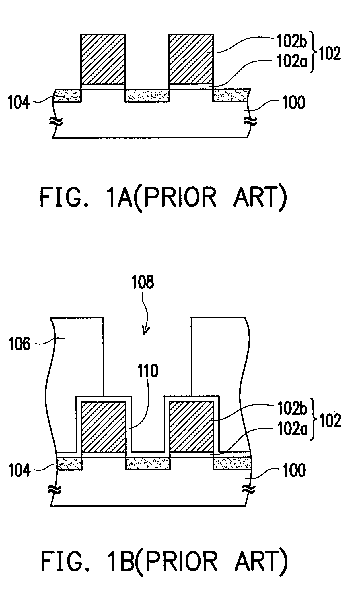
Figure 2 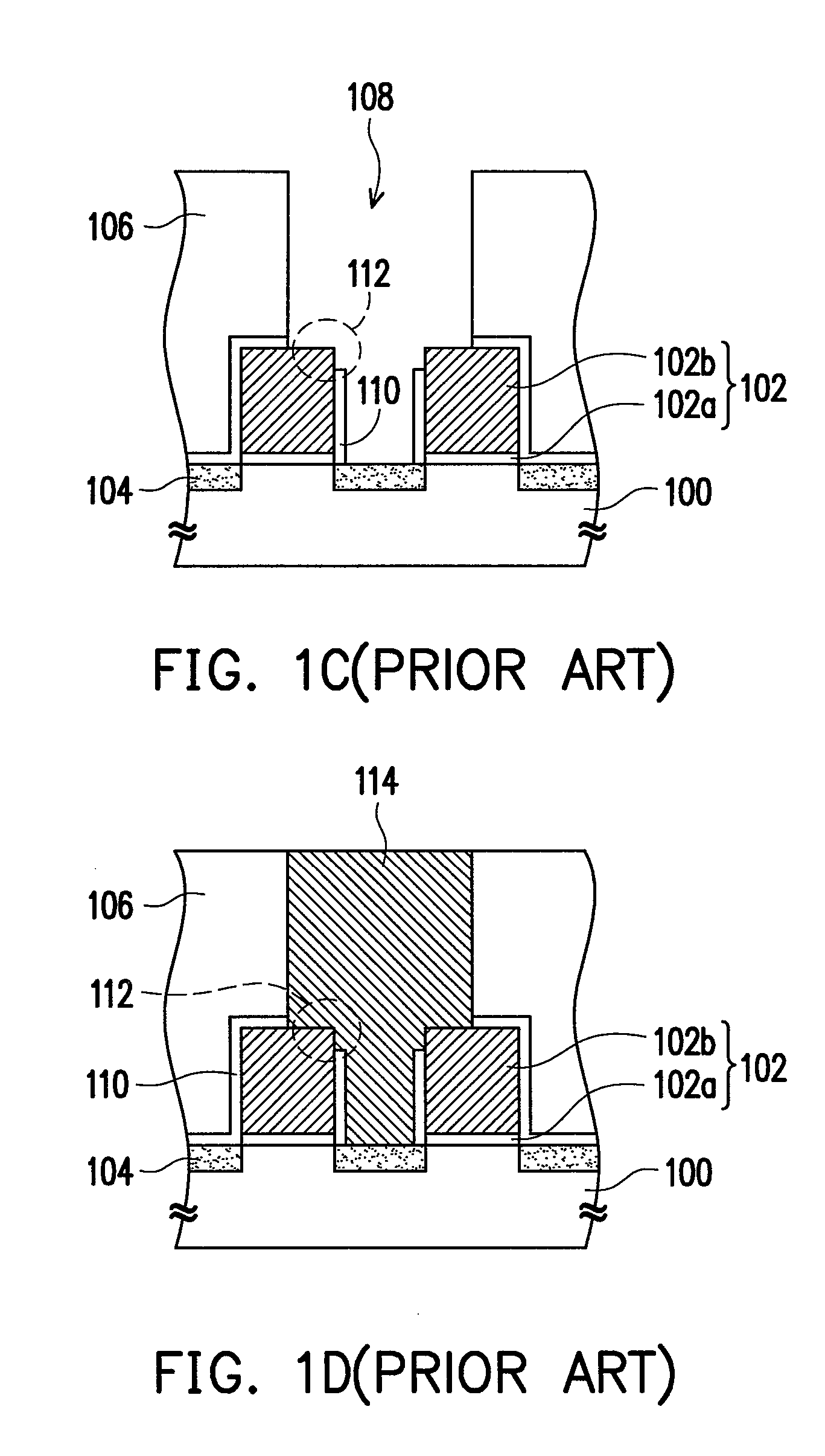
Figure 3
Abstract
Description
CROSS-REFERENCE TO RELATED APPLICATION
[0001] This application claims the priority benefit of Taiwan application serial no. 96136780, filed on Oct. 1, 2007. The entirety of the above-mentioned patent application is hereby incorporated by reference herein and made a part of this specification.BACKGROUND OF THE INVENTION
[0002] 1. Field of the Invention
[0003] The present invention relates to a semiconductor manufacturing process, and more particularly to an interconnect manufacturing process.
[0004] 2. Description of Related Art
[0005] With the progress of semiconductor technology, devices gradually become smaller than ever. When integrity of an integrated circuit (IC) is increased, a surface of a chip cannot provide enough area for placing the required interconnects. In order to meet the requirements of the increased interconnects after the sizes of devices are reduced, a design of multi-layer metal interconnect structure having more than two layers has been inevitably adopted in Very Large S...
Examples
Embodiment Construction
[0030]FIGS. 2A to 2D are cross-sectional views of processes of the interconnect process according to an embodiment of the present invention.
[0031]First, referring to FIG. 2A, a substrate 300 is provided. The substrate 300 has gate structures 302 thereon. Each of the gate structure 302 includes a gate dielectric layer 302a located on the substrate 300 and a gate 302b located on the gate dielectric layer 302a. Moreover, doped regions 304 are disposed in the substrate 300 and respectively located between two adjacent gate structures 302, so as to serve as a source / drain region.
[0032]Referring to FIG. 2B, a liner 310 is conformally formed on the substrate 300. The material of the liner 310 is, for example, silicon oxide, and the liner 310 is formed by, for example, a chemical vapor deposition (CVD) process. A dielectric layer 306 is formed on the substrate 300. The material of the dielectric layer 306 is, for example, silicon oxide, and the dielectric layer 306 is formed by, for example...