
Deinterlacing and film and video detection with configurable downsampling
a deinterlacing and configurable technology, applied in the field of video deinterlacing, can solve the problems of inability to configure and/or flexible use of downsampling/decidation, lack of flexibility in trading off memory bandwidth and quality in the conventional deinterlacers, and loss of quality, so as to save memory bandwidth, reduce resolution fields, and reduce resolution fields
Patent Information
- Authority / Receiving Office
- US · United States
- Patent Type
- Applications(United States)
- Current Assignee / Owner
- Publication Date
- 2009-09-24
Smart Images
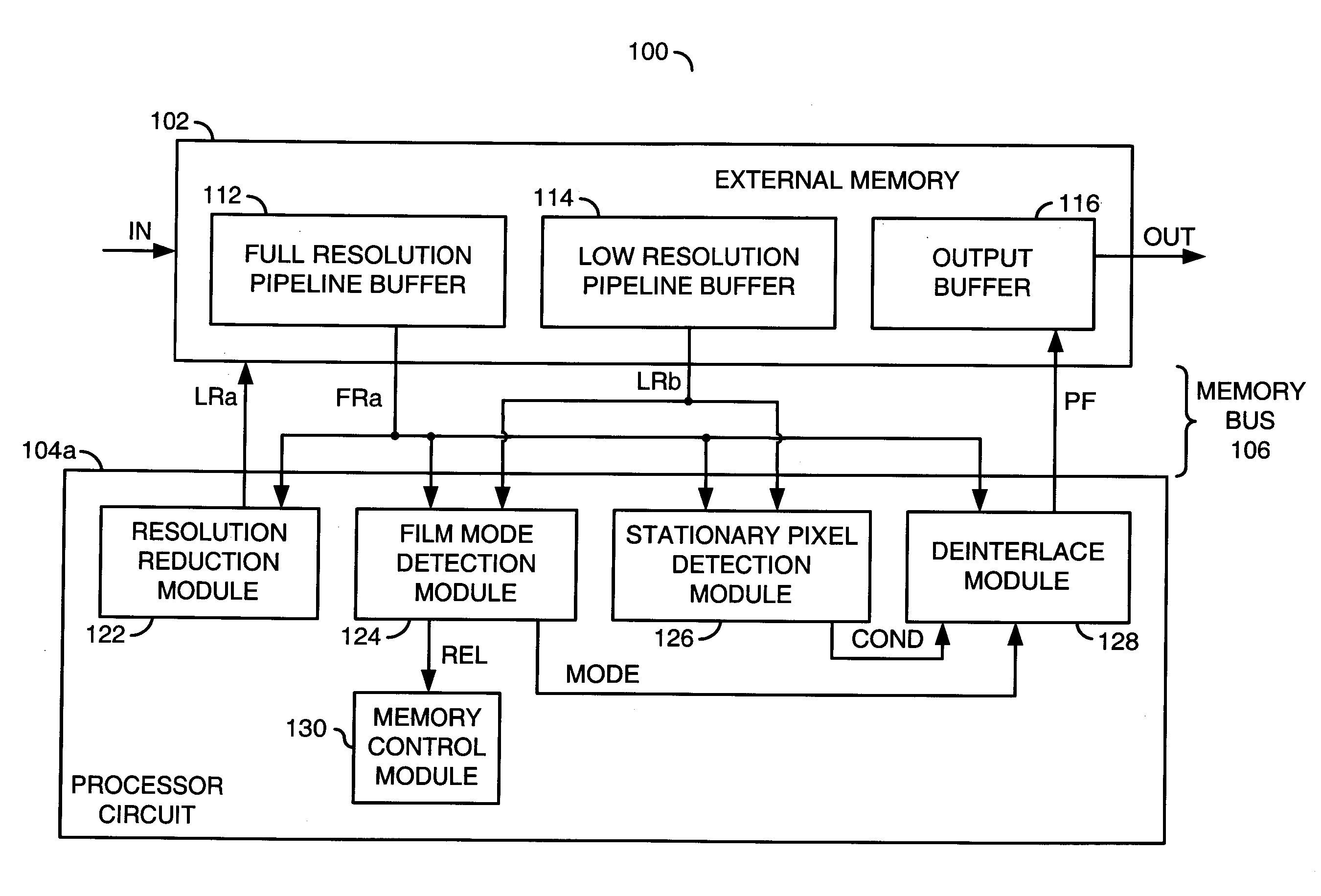
Figure 1 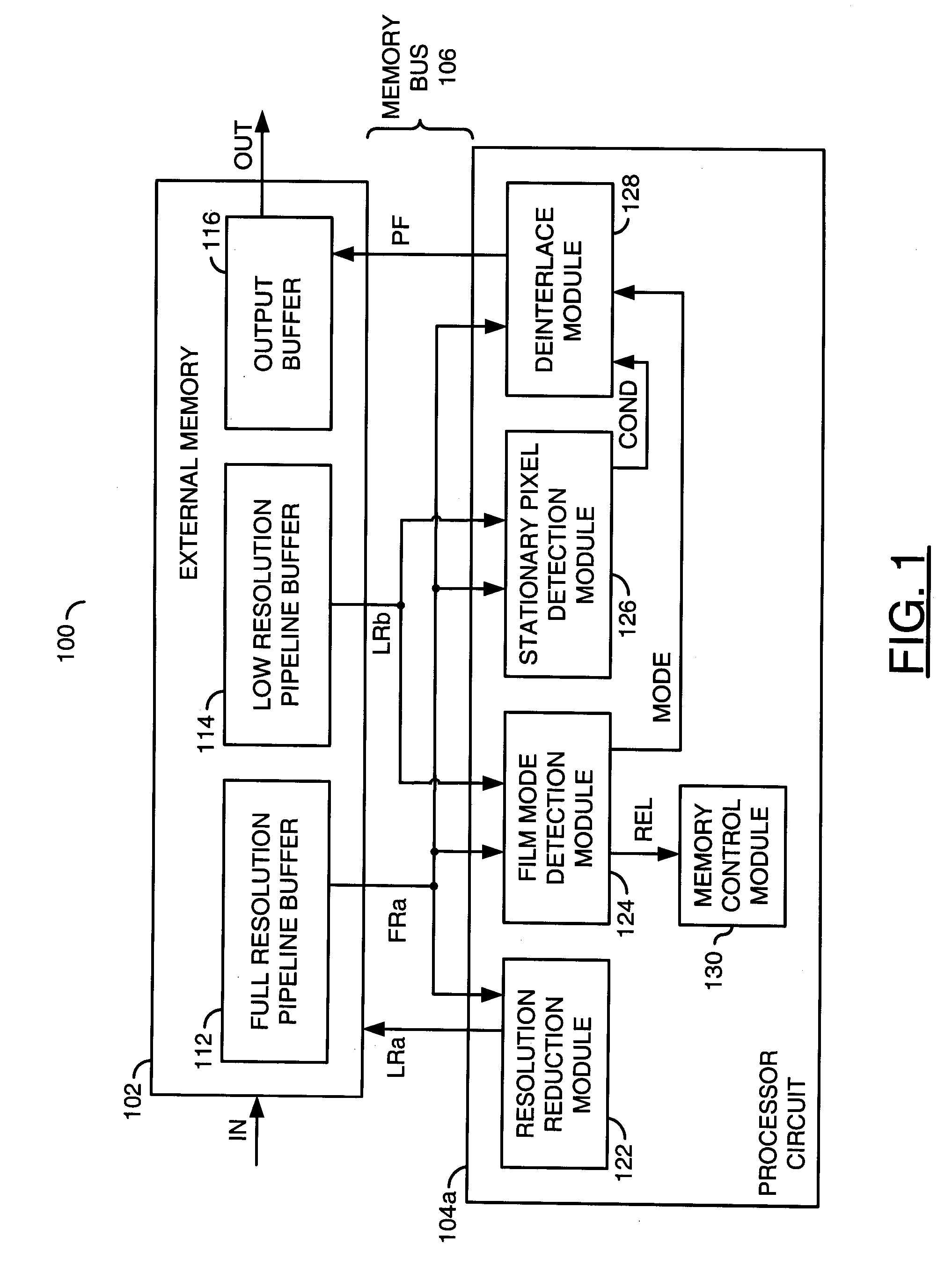
Figure 2 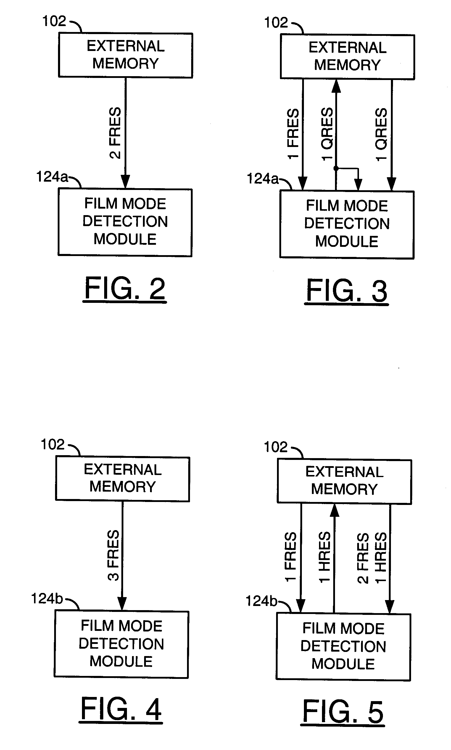
Figure 3
Abstract
Description
FIELD OF THE INVENTION
[0001] The present invention relates to video deinterlacing generally and, more particularly, to a method and / or apparatus for implementing deinterlacing and film and video detection with configurable downsampling.BACKGROUND OF THE INVENTION
[0002] The tasks of video deinterlacing and film-mode detection challenge conventional deinterlacers to achieve a best quality for a minimal memory bandwidth cost. Part of the challenge is a lack of flexibility to trade off memory bandwidth and quality in the conventional deinterlacers. High quality state-of-the-art video deinterlacers use multiple fields of video buffered in a memory to create progressive frames for display. Additionally, high quality state-of-the-art film mode detection units (that are typically used with deinterlacers) use multiple fields from the memory.
[0003] Some existing deinterlacers and conventional film mode detectors are designed to use subsampled or decimated fields to save memory storage and band...
Examples
Embodiment Construction
[0019]Referring to FIG. 1, a block diagram of a first example embodiment of a system 100 is shown in accordance with a preferred embodiment of the present invention. The system (or apparatus) 100 may implement a video deinterlacer. The system 100 is generally operational to deinterlace fields received in an input signal (e.g., IN) and presented progressive frames in an output signal (e.g., OUT). The system 100 generally comprises a memory (or module) 102 and a circuit (or module) 104a in communication with each other through a bus 106. Interlaced fields within the signal IN may be written into the memory 102. The progressive frames may be read from the memory 102 via the signal OUT.
[0020]The memory 102 may be operational to temporarily buffer the interlaced fields and the progressive frames. The memory circuit 102 may be implemented as a single data rate (SDR) dynamic random access memory (DRAM) or a double data rate (DDR) DRAM. Other memory technologies may be implemented to meet t...