

Dielectric film and semiconductor device using dielectric film
a dielectric film and semiconductor technology, applied in the direction of vacuum evaporation coating, transistors, coatings, etc., can solve the problems of hfo/sub>2 formed of a laminated film of tin and hfo/sub>2 also lack heat resistance, and achieve superior heat resistance and flatness, and the relative permittivity of the dielectric film according to the present invention does not decrease.
Patent Information
- Authority / Receiving Office
- US · United States
- Patent Type
- Applications(United States)
- Current Assignee / Owner
- Publication Date
- 2010-12-30
Smart Images
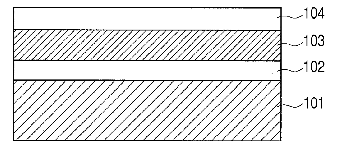
Figure 1 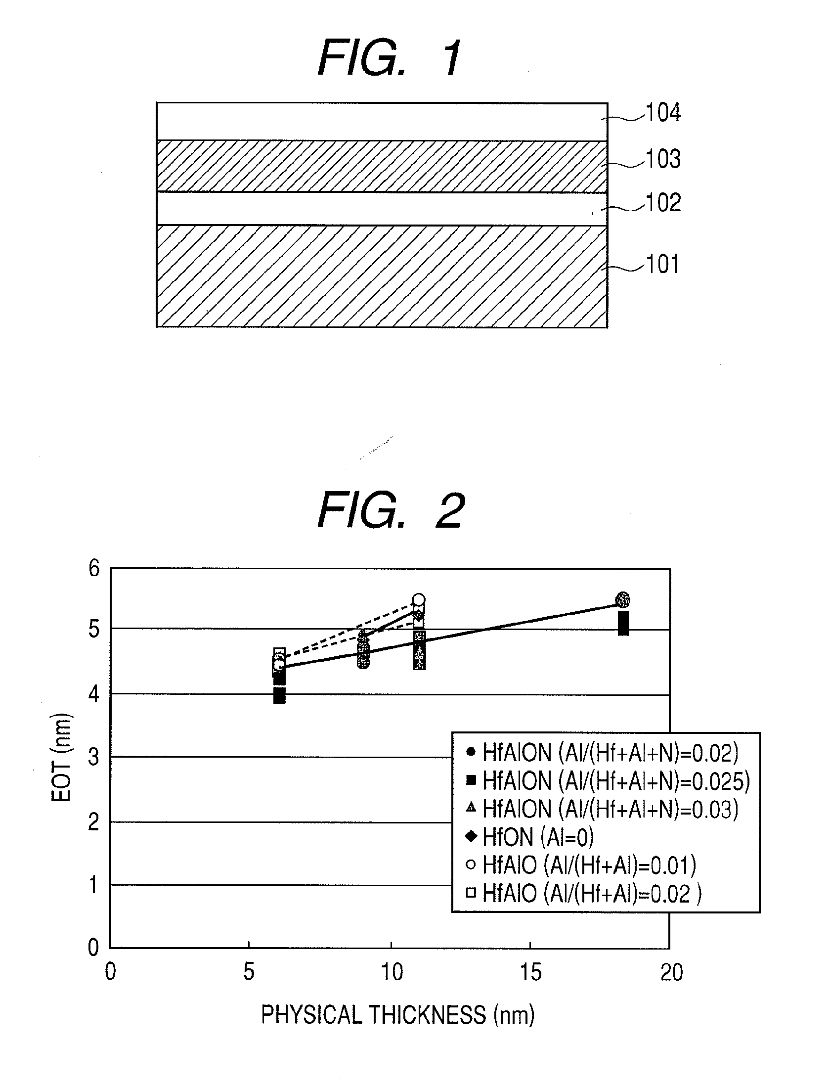
Figure 2 
Figure 3
Abstract
Description
CROSS-REFERENCES TO RELATED APPLICATIONS
[0001] This application is a continuation application of International Application No. PCT / JP2009 / 065305, filed on Sep. 2, 2009, the entire contents of which are incorporated by reference herein.
[0002] This application also claims the benefit of priority from Japanese Patent Application No. 2008-282100 filed Oct. 31, 2008, the entire contents of which are incorporated herein by reference.TECHNICAL FIELD
[0003] The present invention relates to a dielectric film and a semiconductor device using a dielectric film.BACKGROUND ART
[0004] Developments in semiconductor devices are accompanied by increasingly higher degrees of element integration, resulting in increased miniaturization of each element and a reduction in operating voltage. For example, in the field of MONOS (metal oxide nitride oxide semiconductor)-type non-volatile semiconductor devices which include a blocking film that separates a charge retaining layer and a gate electrode, the miniaturiz...
Examples
first example (
Example Using Cosputtering)
[0103]A first example of the present invention will now be described in detail with reference to the drawings.
[0104]FIG. 1 is a diagram illustrating an MIS capacitor having the dielectric film 103. A HfAlON film was deposited by a sputtering method as the dielectric film 103 on the silicon substrate 101 having the silicon dioxide film 102 with a film thickness of 3 to 5 nm on a surface thereof. Metallic targets of Hf and Al were used as targets. Argon, oxygen, and nitrogen were used as sputter gases. In other words, a substrate processing apparatus according to the present example includes, in a first chamber thereof, a supplying mechanism that supplies a Hf target, an Al target, and a sputter gas into the first chamber. More specifically, the substrate processing apparatus according to the present example includes a first physical vapor deposition mechanism for performing physical vapor deposition such as sputtering using a Hf target and an Al target.
[010...
second example (
Example Using ALD Method and CVD Method)
[0124]The present example differs from the first example in that the dielectric film 103 is formed by a CVD method or an ALD method. Other formation processes are the same as the first example. Therefore, a substrate processing apparatus according to the present example includes a mechanism for realizing at least one of a CVD method and an ALD method such as a supplying mechanism that supplies an organic metallic material and an oxidant into a chamber.
[0125]A HfAlON film was formed as the dielectric film 103 by a CVD method or an ALD method at a range of 5 nm to 25 nm on the substrate 101 having the silicon dioxide film 102 on a surface thereof. A substrate temperature was set to 300° C., trimethylaluminum (Al(CH3)3) and tetrakis(diethylamino)hafnium (Hf[(C2H5)2N]4) were used as organic metallic materials, and H2O was used as an oxidant. The method of forming a dielectric film can be set by controlling a partial pressure of the oxidant to be i...
third example (
Example Applied to Gate Insulating Film)
[0137]A third example of the present invention will now be described in detail with reference to the drawings.
[0138]FIG. 16 is a diagram illustrating processes of a semiconductor device manufacturing method according to a third example of the present invention.
[0139]First, as depicted by process 1 in FIG. 16, a substrate processing apparatus according to the present example forms an element isolation region 302 on a surface of a silicon substrate 301 using a STI (shallow trench isolation) technique. The substrate processing apparatus according to the present example then forms a silicon dioxide film 303 with a film thickness of 1.8 nm on the element-isolated surface of the silicon substrate using a thermal oxidation method. Subsequently, the substrate processing apparatus according to the present example forms a HfAlON film with a film thickness ranging from 1 nm to 10 nm as a dielectric film 304 using the same method as the first example or t...