
Mixer-transconductance interface
Patent Information
- Authority / Receiving Office
- US · United States
- Current Assignee / Owner
- Publication Date
- 2011-01-06
- Estimated Expiration
- Not applicable · inactive patent
Smart Images
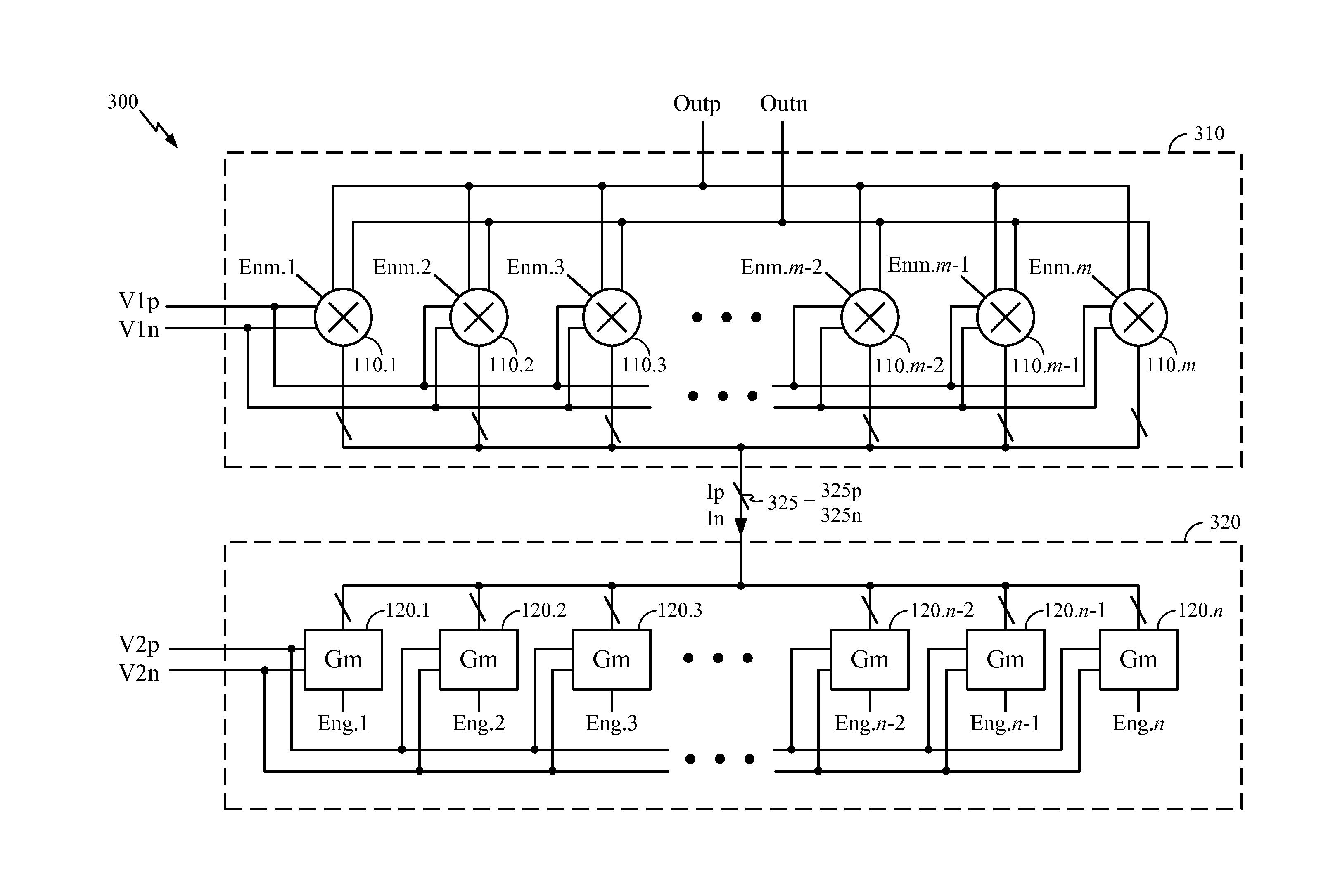
Figure 1 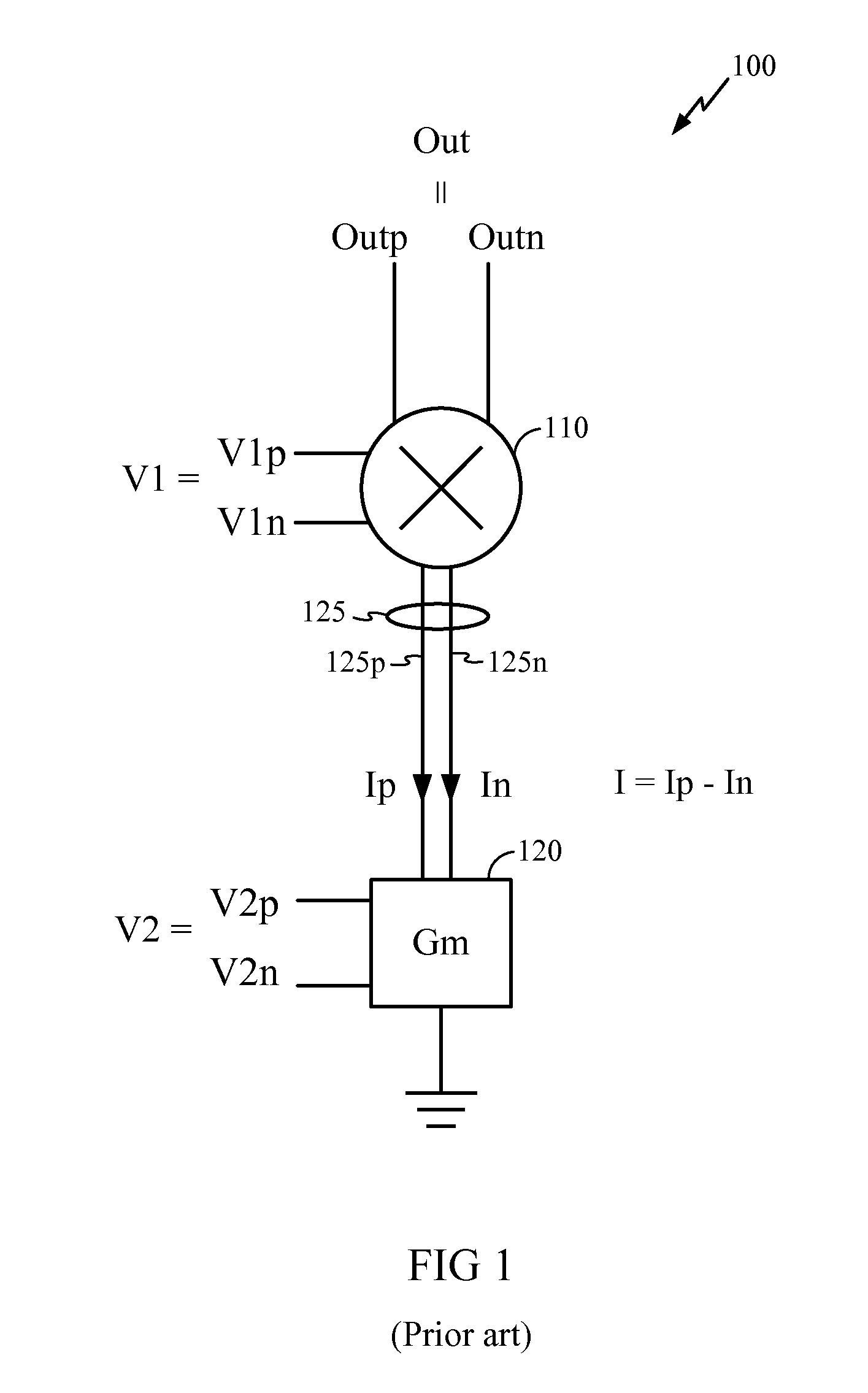
Figure 2 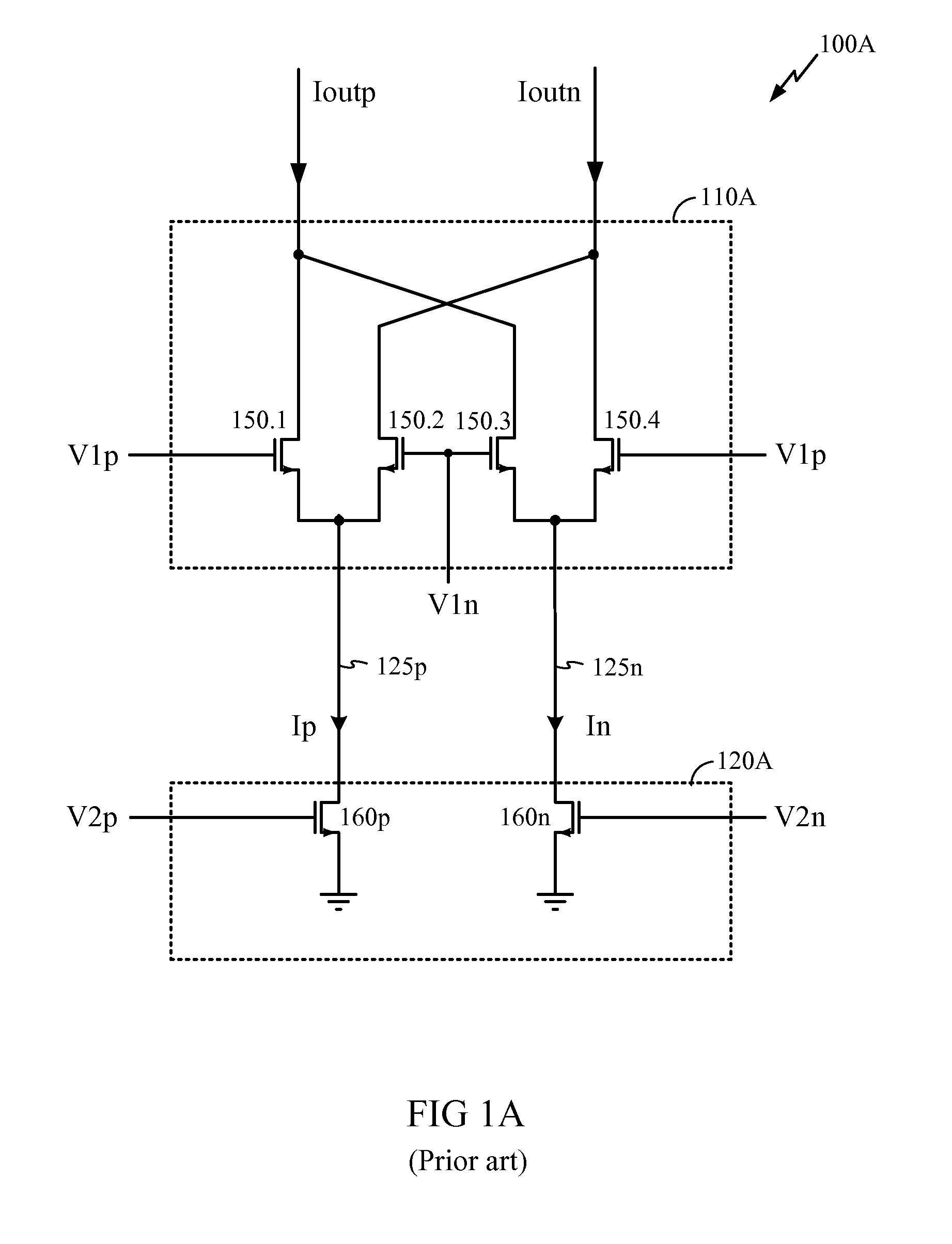
Figure 3
Abstract
Description
BACKGROUND1. FieldThe disclosure relates to circuit design, and in particular, to an efficient mixer-transconductance interface.2. BackgroundCommunications circuitry may employ one or more mixer circuits to translate a signal spectrum from one frequency to another frequency. For example, in a transmitter, a mixer may be used in an upconverter to convert a baseband signal to a radio-frequency (RF) signal. In a receiver, a mixer may be used in a downconverter to convert a received RF signal to an intermediate frequency (IF) or baseband for processing. Certain mixer circuits may utilize a current-mode architecture wherein a first input voltage is mixed with a signal current, e.g., a bias current of the mixer, to generate an output signal. The signal current may be generated by a transconductance (Gm) block, which in turn generates the signal current from a second input voltage. In some implementations, both the mixer and the Gm block may be provided with multiple gain settings to tune ...
Examples
exemplary embodiment 300
FIG. 3 illustrates an exemplary embodiment 300 of a gain-controlled mixer-transconductance block according to the present disclosure. In FIG. 3, the Ip outputs of the n Gm unit cells 120.1 through 120.n are conductively coupled together, and the In outputs of the n Gm unit cells are also conductively coupled together. In this specification and in the claims, the term “conductively coupled” shall denote the condition wherein an electrical short circuit, i.e., a conductive path of low electrical resistance, exists between the coupled nodes.
The sum of the Ip currents is carried on a single conductive lead 325p, and the sum of the In currents is carried on a single conductive lead 325n. The two conductive leads 325p and 325n are collectively labeled as the conductive path 325 in FIG. 3. At the mixer, the leads 325p and 325n are each coupled to the individual current inputs of the mixer unit cells 110.1 through 110.m. The conductive leads 325p and 325n may be understood as being fanned o...
exemplary embodiment 400
In an exemplary embodiment, the techniques described herein may further accommodate transceivers utilizing a quadrature mixing scheme. FIG. 4 illustrates an exemplary embodiment 400 of a mixer-transconductance block for mixing two complex signals with each other. In FIG. 4, the mixer-transconductance block 400 is configured to mix in-phase and quadrature differential local oscillator voltages (LO_Ip, LO_In, LO_Qp, LO_Qn) with in-phase and quadrature differential voltages (V_Ip, V_In, V_Qp, V_Qn) corresponding to a received signal or signal to be transmitted. Note in FIG. 4 that the enable signals for the mixer unit cells (not shown) are labeled Enm.1 . . . . Enm.m (I) for the in-phase voltages and Enm.1 . . . Enm.m (Q) for the quadrature voltages, while enable signals for the Gm unit cells (also not shown) are labeled Eng.1 . . . Eng.n (I) for the in-phase voltages and Eng.1 . . . Eng.n (Q) for the quadrature voltages.
In the embodiment 400, separate conducting paths are provided to ...