
Beamlet blanker arrangement
Patent Information
- Authority / Receiving Office
- US · United States
- Current Assignee / Owner
- Publication Date
- 2012-04-19
Smart Images
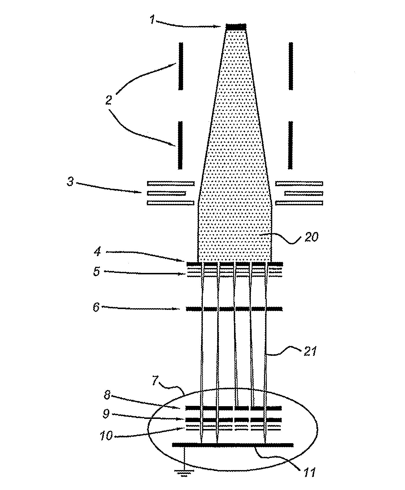
Figure 1 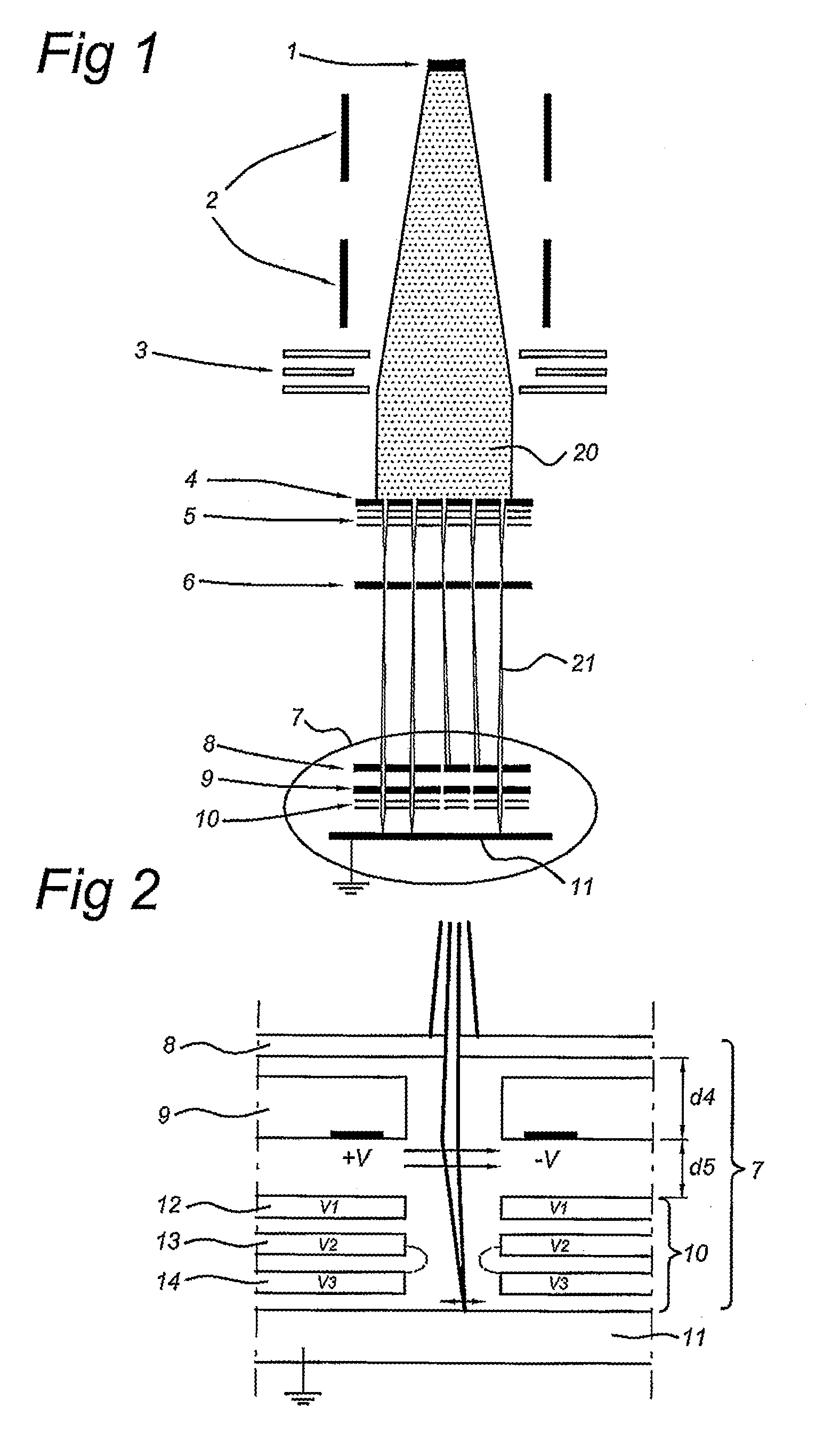
Figure 2 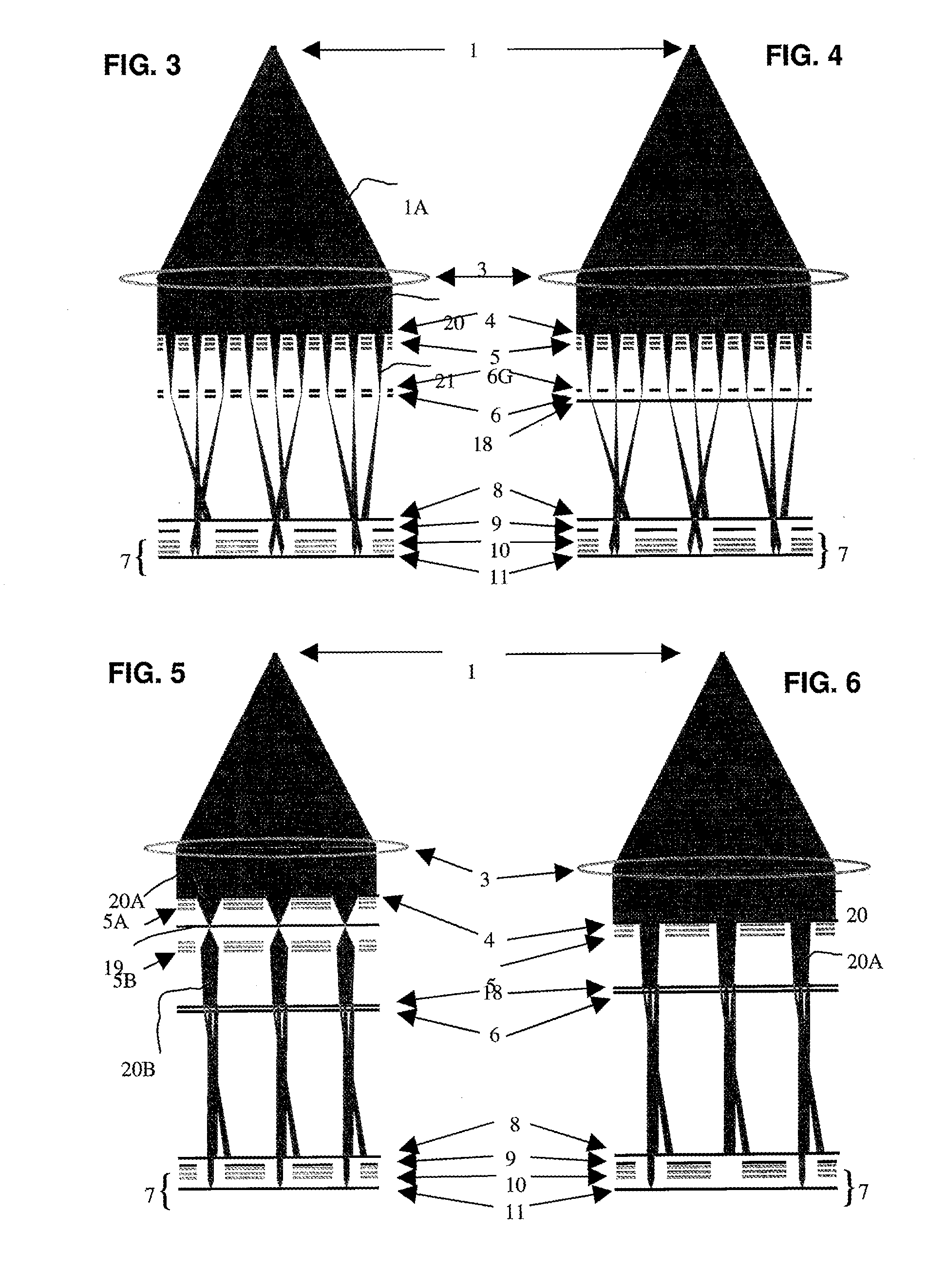
Figure 3
Abstract
Description
BACKGROUND OF THE INVENTION
[0001] 1. Field of the Invention
[0002] The present invention relates to a projection system for a charged particle multi-beamlet system, such as for a charged particle multi-beamlet lithography system or an inspection system, and an end module for such a projection system.
[0003] The present invention more specifically relates to a deflection device, in particular a beamlet blanker for use in a charged particle multi-beamlet lithography system, the blanker comprising a substrate provided with apertures and deflectors with a first electrode and a second electrode arranged around an aperture, the deflectors receiving electrical signals for deflecting beamlets of charged particles passing through the apertures.
[0004] The present invention further relates to a charged particle multi-beamlet lithography system, to a deflecting method and a method of transferring a pattern to a target surface.
[0005] 2. Description of the Related Art
[0006] Currently, most commercial lit...
Examples
Embodiment Construction
[0079]The following is a description of various embodiments of the invention, given by way of example only and with reference to the drawings.
[0080]FIG. 1 shows a simplified schematic drawing of an embodiment of a charged particle multi-beamlet lithography system based upon an electron beam optical system without a common cross-over of all the electron beamlets. Such lithography systems are described for example in U.S. Pat. Nos. 6,897,458 and 6,958,804 and 7,084,414 and 7,129,502 which are all hereby incorporated by reference in their entirety, assigned to the owner of the present invention. In the embodiment shown in FIG. 1, the lithography system comprises an electron source 1 for producing a homogeneous, expanding electron beam 20. Beam energy is preferably maintained relatively low in the range of about 1 to 10 keV. To achieve this, the acceleration voltage is preferably low, the electron source preferably kept at between about −1 to −10 kV with respect to the target at ground ...