
Input device and method of manufacturing input device
Patent Information
- Authority / Receiving Office
- US · United States
- Current Assignee / Owner
- Publication Date
- 2012-09-13
- Estimated Expiration
- Not applicable · inactive patent
Smart Images
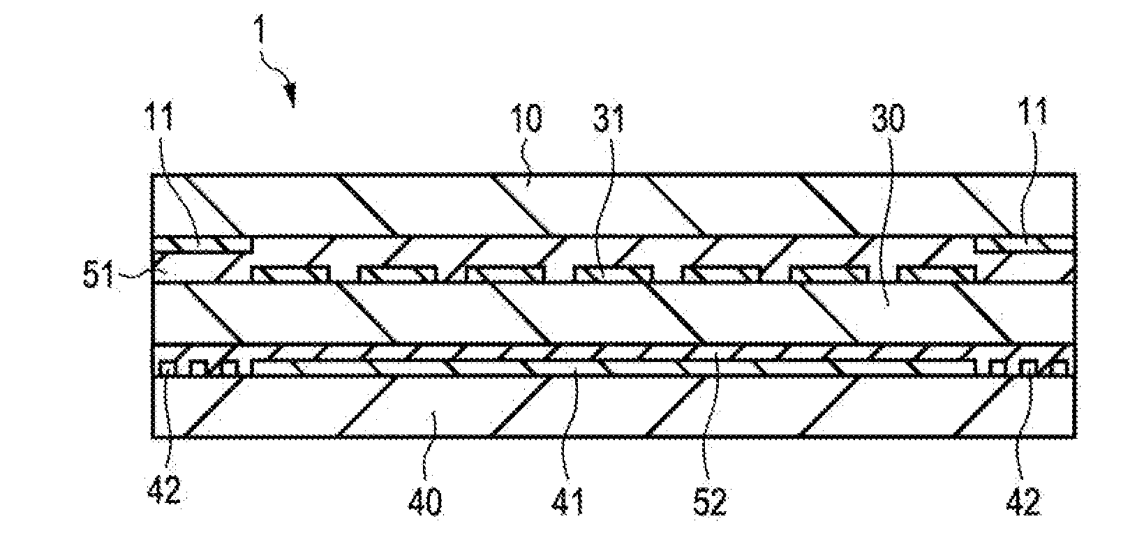
Figure 1 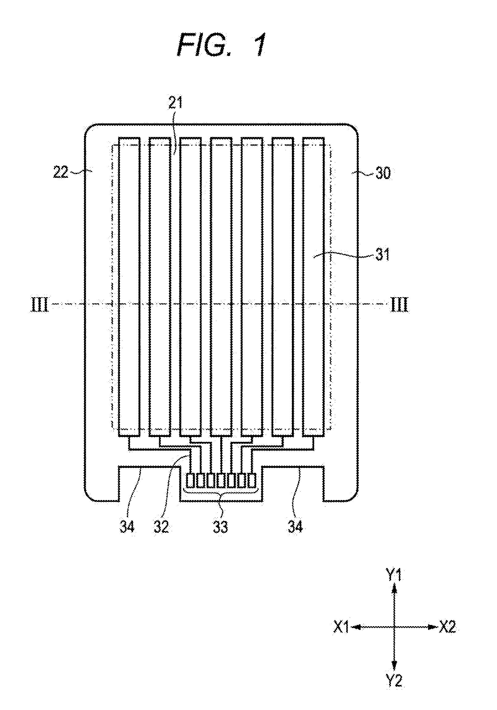
Figure 2 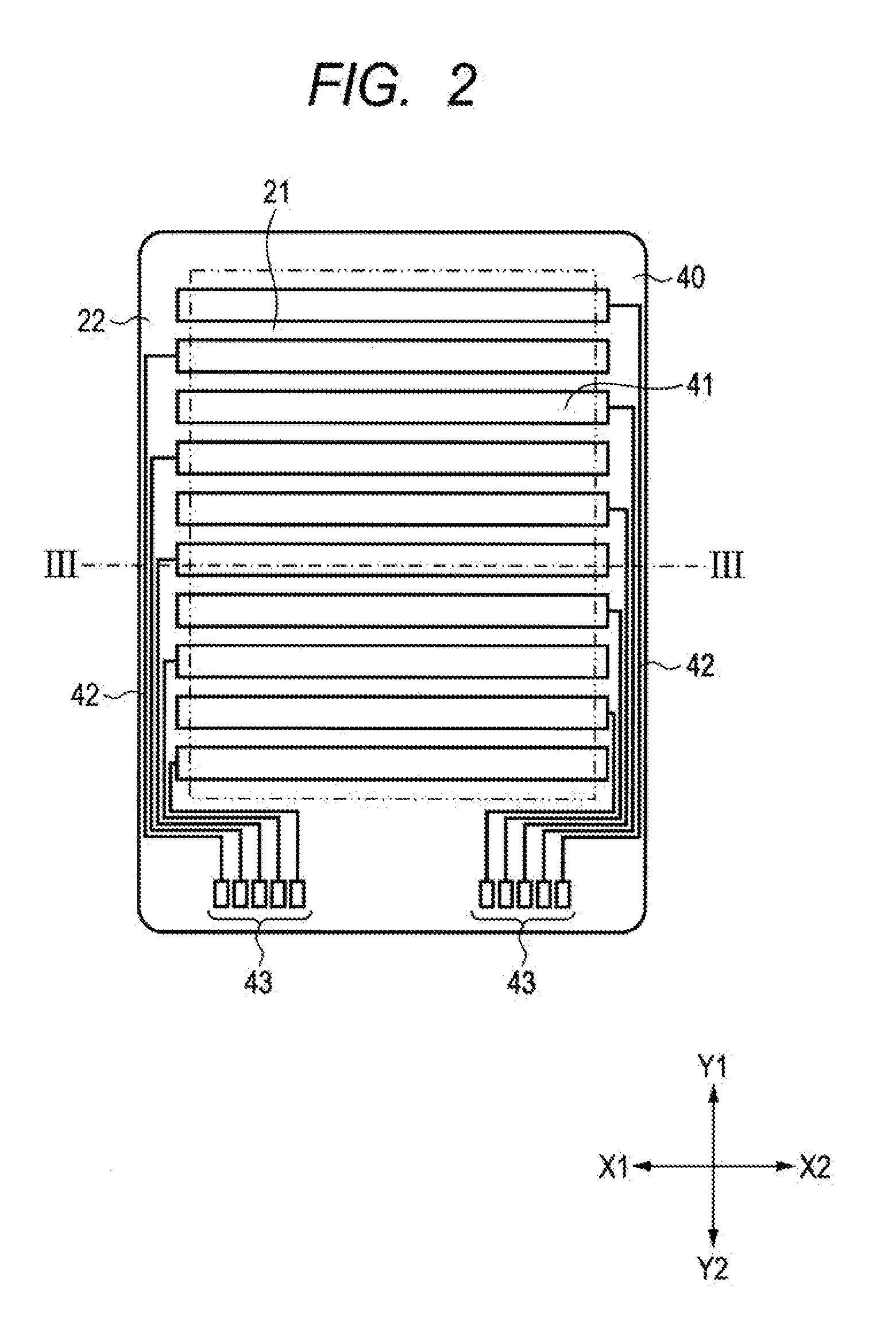
Figure 3
Abstract
Description
CLAIM OF PRIORITY
[0001] This application claims benefit of Japanese Patent Application No. 2011-050942 filed on Mar. 9, 2011, which is hereby incorporated by reference.BACKGROUND OF THE INVENTION
[0002] 1. Field of the Invention
[0003] The present invention relates to an input device and a method of manufacturing the input device, and more particularly, to an input device that can improve environmental resistance and a method of manufacturing the input device.
[0004] 2. Description of the Related Art
[0005] Currently, a translucent input device is used as a display portion of an electronic device such as a mobile phone. An input device is disposed so as to overlap a display device such as liquid crystal, and a user can be in visual contact with an image, which is displayed on the display device, through the input device. Further, a user can input position information by touching an input region with a finger or an input tool.
[0006] There are several types as the operation type of the input de...
Examples
first embodiment
[0039]FIG. 1 is a plan view of a first transparent base 30 of an input device 1 according to a first embodiment. FIG. 2 is a plan view of a second transparent base 40 of the input device 1 according to the first embodiment. Further, FIG. 3 is a cross-sectional view of the input device 1, where the respective transparent bases and a surface member 10 are laminated and assembled, taken along a line III-III of FIGS. 1 and 2.
[0040]As shown in FIG. 1, a first transparent electrode layer 31, first lead electrodes 32, and first connection electrodes 33 are formed on one surface of the first transparent base 30. As shown in FIG. 1, the first transparent electrode layer 31 is formed of a plurality of strip-shaped bodies extending in a Yl-Y2 direction and the plurality of strip-shaped bodies are arranged parallel to each other at intervals in an X1-X2 direction.
[0041]The first transparent electrode layer 31 is formed in an input region 21 of the first transparent base 30, and a frame-like non...
second embodiment
[0069]FIG. 9 is a schematic plan view of the vicinity of a connecting portion of an input device 1 according to a second embodiment that is to be connected to an FPC 63. FIG. 10 is a schematic cross-sectional view of the input device 1 taken along a line X-X of FIG. 9. Meanwhile, the same components as the components of the first embodiment are denoted by the same reference numerals and the detailed description thereof will be omitted.
[0070]As in the first embodiment, in the input device 1 according to this embodiment, first and second transparent bases 30 and 40 and a surface member 10 are laminated with first and second optical adhesive layers 51 and 52 interposed therebetween. Further, a transparent electrode layer, lead electrodes, and connection electrodes are formed on each of the first and second transparent bases 30 and 40.
[0071]As shown in FIGS. 9 and 10, the first optical adhesive layer 51 and the FPC 63 are disposed on one surface of the first transparent base 30 with a p...