
Optical Fibers Functionalized with Photonic Crystal Resonant Optical Structures
a technology of optical fibers and photonic crystals, applied in the field of optical fibers functionalized with photonic crystal resonant optical structures, can solve the problems of difficult integration in large systems with many devices, difficult coupling of light on and off-chip, and no optical fiber has demonstrated functional cavities coupled to the tip of optical fibers, etc., to achieve simple and durable construction, tight space, and easy to mak
Patent Information
- Authority / Receiving Office
- US · United States
- Patent Type
- Applications(United States)
- Current Assignee / Owner
- Publication Date
- 2013-02-14
- Estimated Expiration
- Not applicable · inactive patent
Smart Images
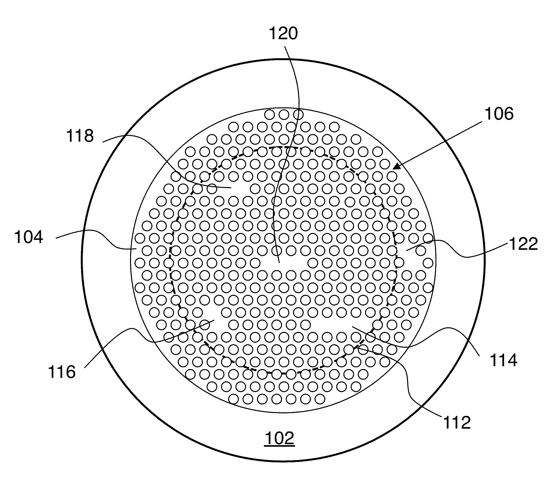
Figure 1 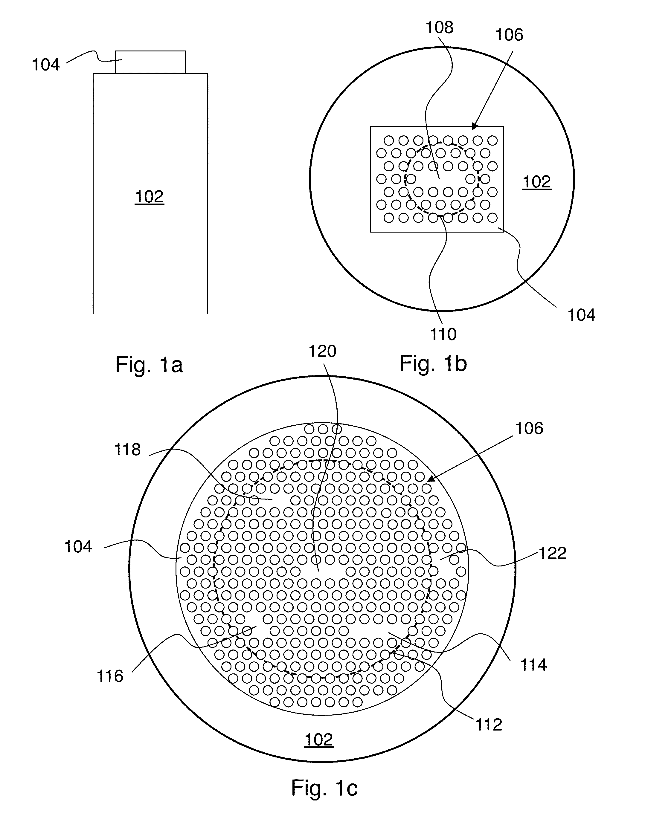
Figure 2 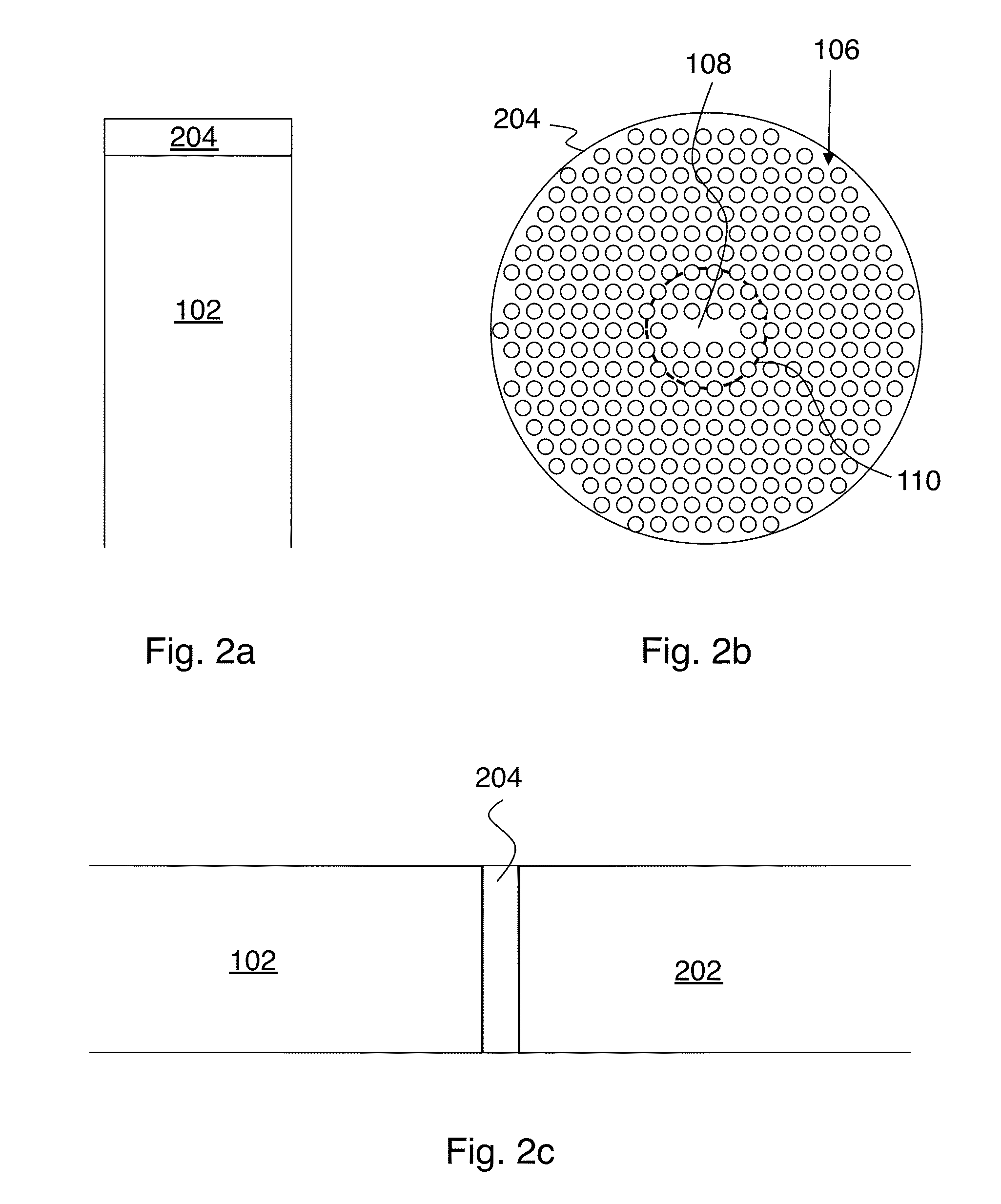
Figure 3
Abstract
Description
CROSS REFERENCE TO RELATED APPLICATIONS
[0001] This application claims the benefit of U.S. provisional patent application 61 / 574,750, filed on Aug. 8, 2011, entitled “Optical Fibers Functionalized with Photonic Crystal Cavities”, and hereby incorporated by reference in its entirety.FIELD OF THE INVENTION
[0002] This invention relates to fiber-coupled photonic crystal devices.BACKGROUND
[0003] A photonic crystal (PC) has a periodic array of features (e.g., holes) in a background medium. Various devices can be fabricated by modifying the basic structure of a photonic crystal. For example, a PC cavity can be formed by a small cluster of missing holes in a PC lattice (effectively forming a point defect in the PC). As another example, a PC waveguide can be formed by a line of missing holes in a PC lattice.
[0004] Photonic crystal devices can readily be fabricated on various semiconducting and / or dielectric substrates. However, it is often difficult to efficiently couple to the resulting PC devic...
Examples
Embodiment Construction
[0048]In this description, section A provides a description of principles relating to various embodiments of the invention, and section B describes some experimental results.
A) Principles
[0049]FIGS. 1a-c show some embodiments of the invention. FIG. 1a shows a side view and FIG. 1b shows a corresponding top view. Here a device 104 is affixed to an exposed end face of optical fiber 102. Device 104 includes at least one resonant optical structure (e.g., cavity 108) defined by a photonic crystal structure 106 in a semiconducting or dielectric material. Fiber 102 is optically coupled to cavity 108 (e.g., by providing a spatial overlap of the fiber core 110 and cavity 108). As described in detail below, device 104 is fabricated on a substrate distinct from fiber 102, and then transferred to fiber 102. FIG. 1c shows a variant. Here fiber core 112 overlaps with several cavities (114, 116, 118, 120), and cavity 122 does not overlap with the core. Instead, cavity 122 is aligned with the cladd...