
Chip device, multi-layered chip device and method of producing the same
Patent Information
- Authority / Receiving Office
- US · United States
- Current Assignee / Owner
- Publication Date
- 2014-01-23
- Estimated Expiration
- Not applicable · inactive patent
Smart Images
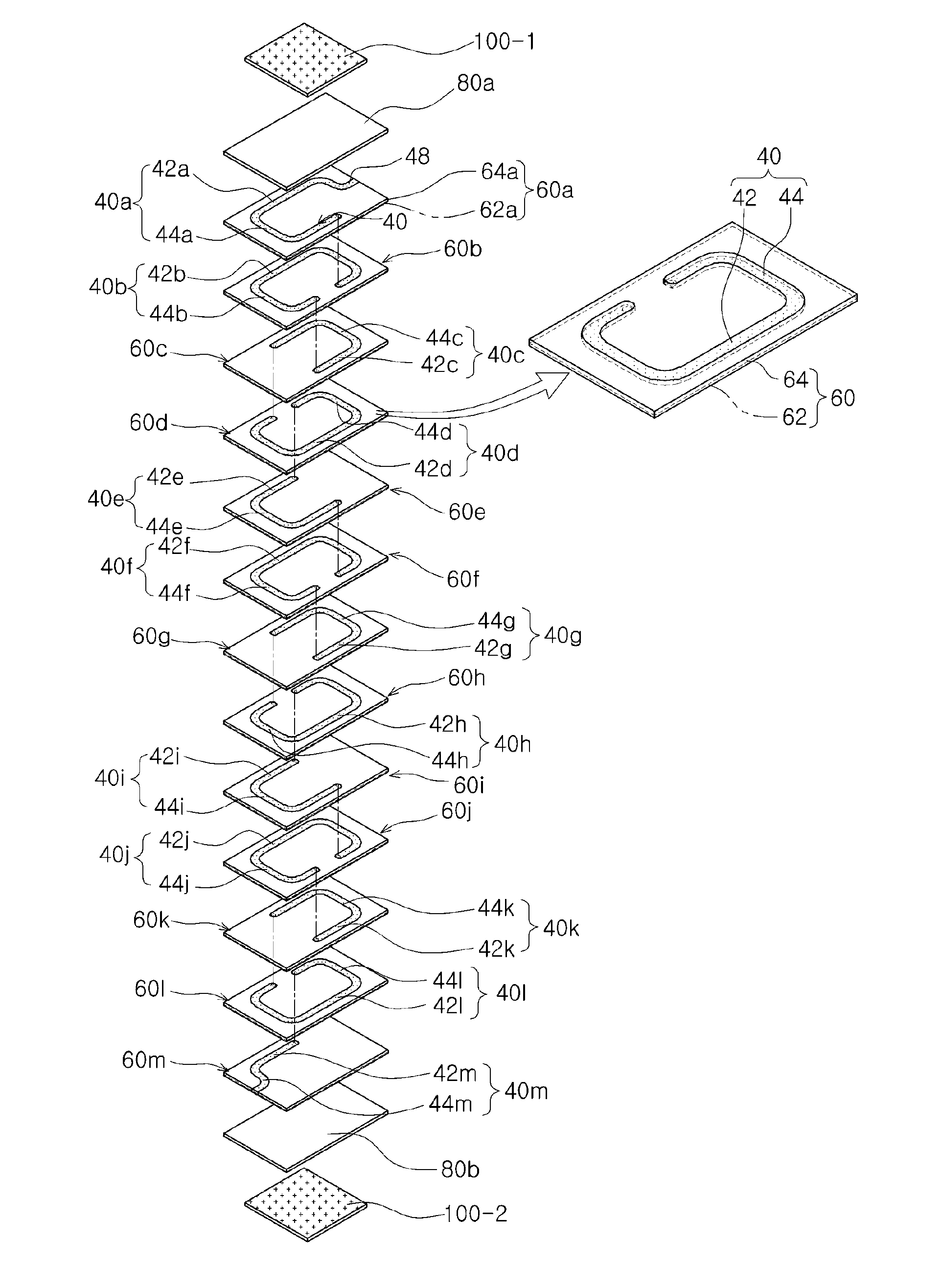
Figure 1 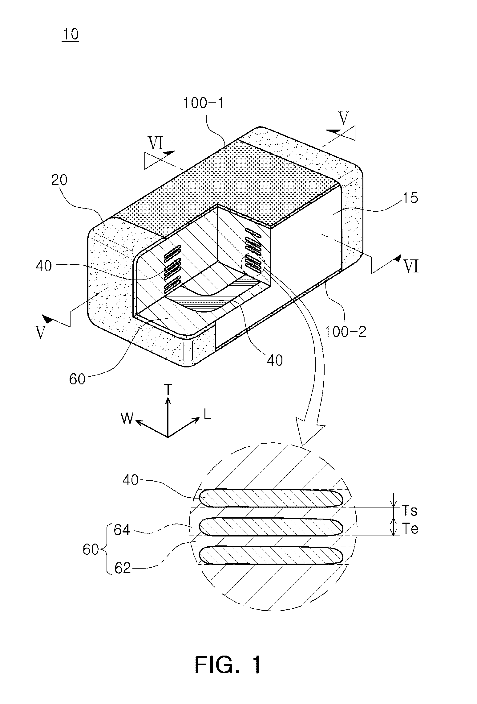
Figure 2 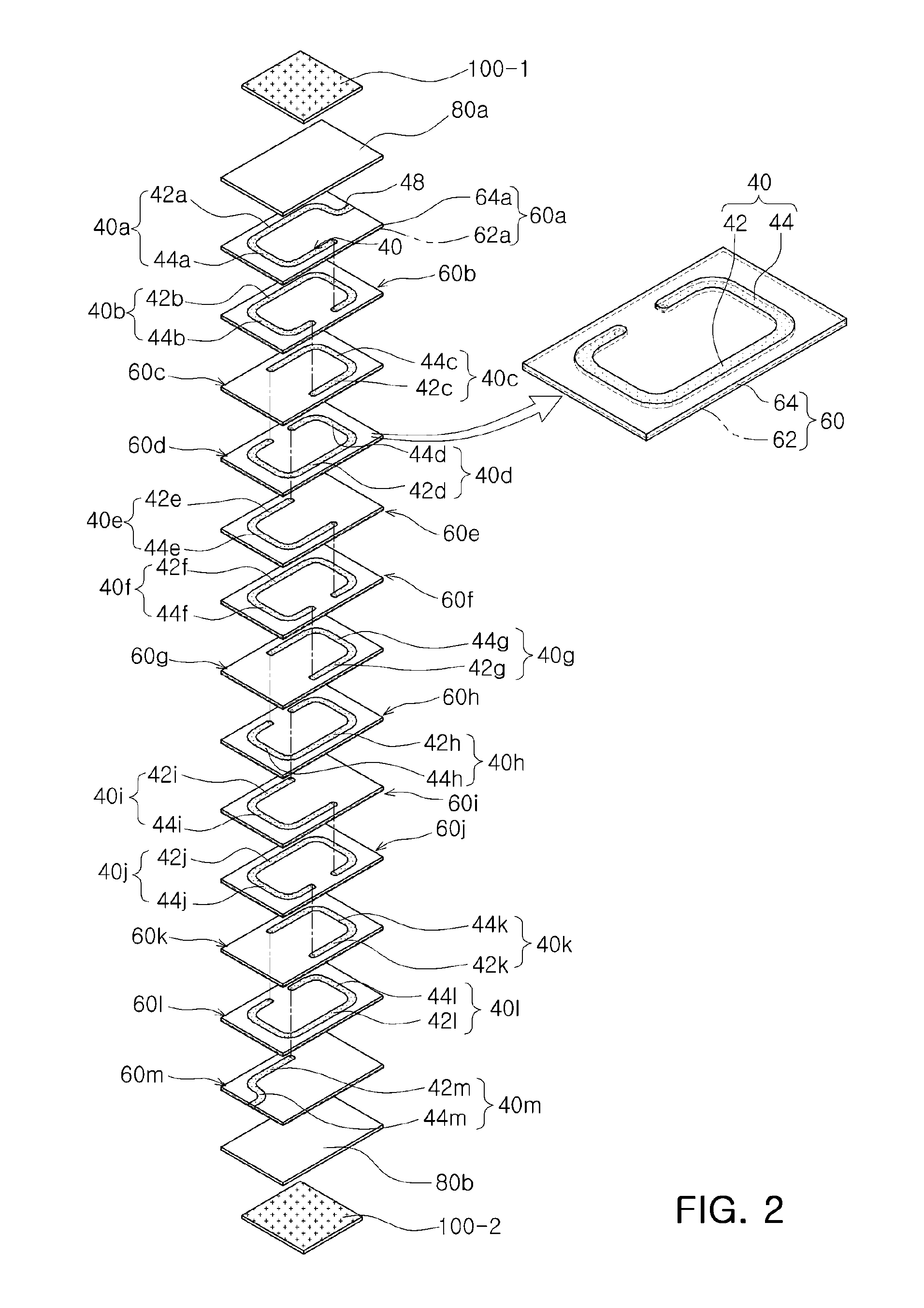
Figure 3
Abstract
Description
CROSS-REFERENCE TO RELATED APPLICATIONS
[0001] This application claims the priority of Korean Patent Application No. 10-2012-0078422 filed on Jul. 18, 2012, in the Korean Intellectual Property Office, the disclosure of which is incorporated herein by reference.BACKGROUND OF THE INVENTION
[0002] 1. Field of the Invention
[0003] The present invention relates to a chip device, a multi-layered chip device, and a method of producing the same.
[0004] 2. Description of the Related Art
[0005] An inductor, a multi-layered chip component, is a representative passive element capable of removing noise from a signal by being included in an electronic circuit together with a resistor and a capacitor.
[0006] A multi-layered chip type inductor may be manufactured by printing and stacking conductive patterns so as to form a coil within a magnetic substance or a dielectric substance. The multi-layered chip inductor has a structure in which a plurality of magnetic layers on which conductive patterns are formed ar...
Examples
Embodiment Construction
[0025]Hereinafter, embodiments of the present invention will be described in detail with reference to the accompanying drawings. The invention may, however, be embodied in many different forms and should not be construed as being limited to the embodiments set forth herein. Rather, these embodiments are provided so that this disclosure will be thorough and complete, and will fully convey the scope of the invention to those skilled in the art. In the drawings, the shapes and dimensions of elements may be exaggerated for clarity, and the same reference numerals will be used throughout to designate the same or like elements.
[0026]In addition, singular forms used in the specification are intended to include plural forms unless the context clearly indicates otherwise. In the specification, it is to be noted that the terms “comprising” or “including”, and the like, are not to be construed as necessarily including several components or several steps described in the specification, and some...