
Solar cell
a solar cell and cell technology, applied in the field of solar cells, can solve the problems of degrading the efficiency of the solar cell and a pattern defect, and achieve the effect of minimizing the loss of efficiency
Patent Information
- Authority / Receiving Office
- US · United States
- Patent Type
- Applications(United States)
- Current Assignee / Owner
- Publication Date
- 2015-05-21
- Estimated Expiration
- Not applicable · inactive patent
Smart Images
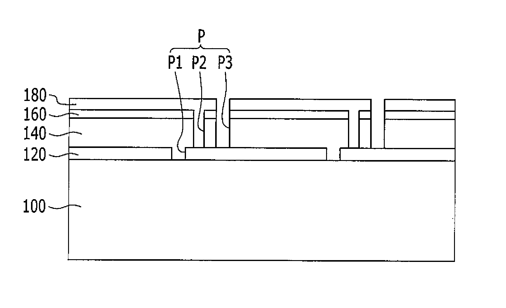
Figure 1 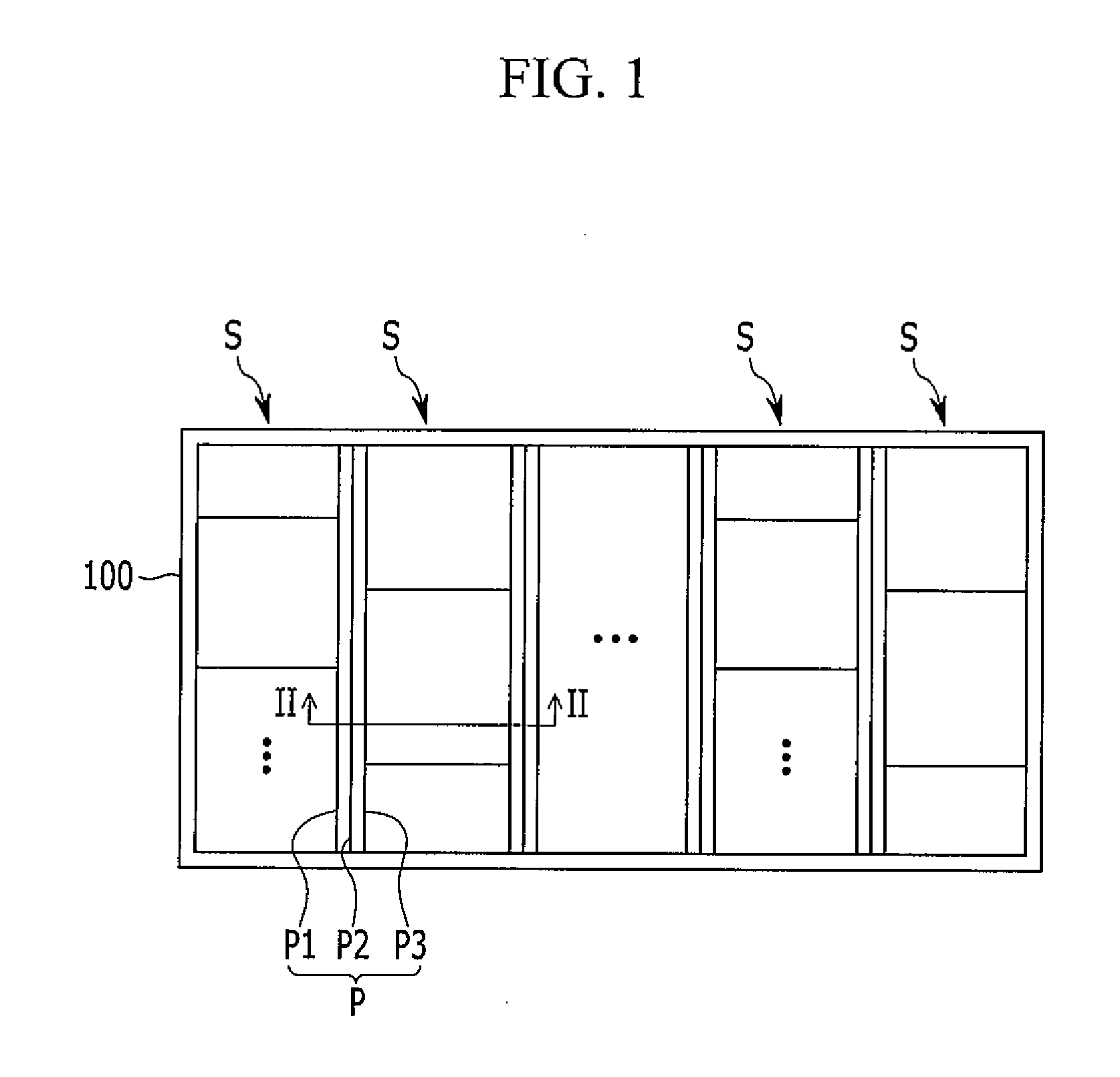
Figure 2 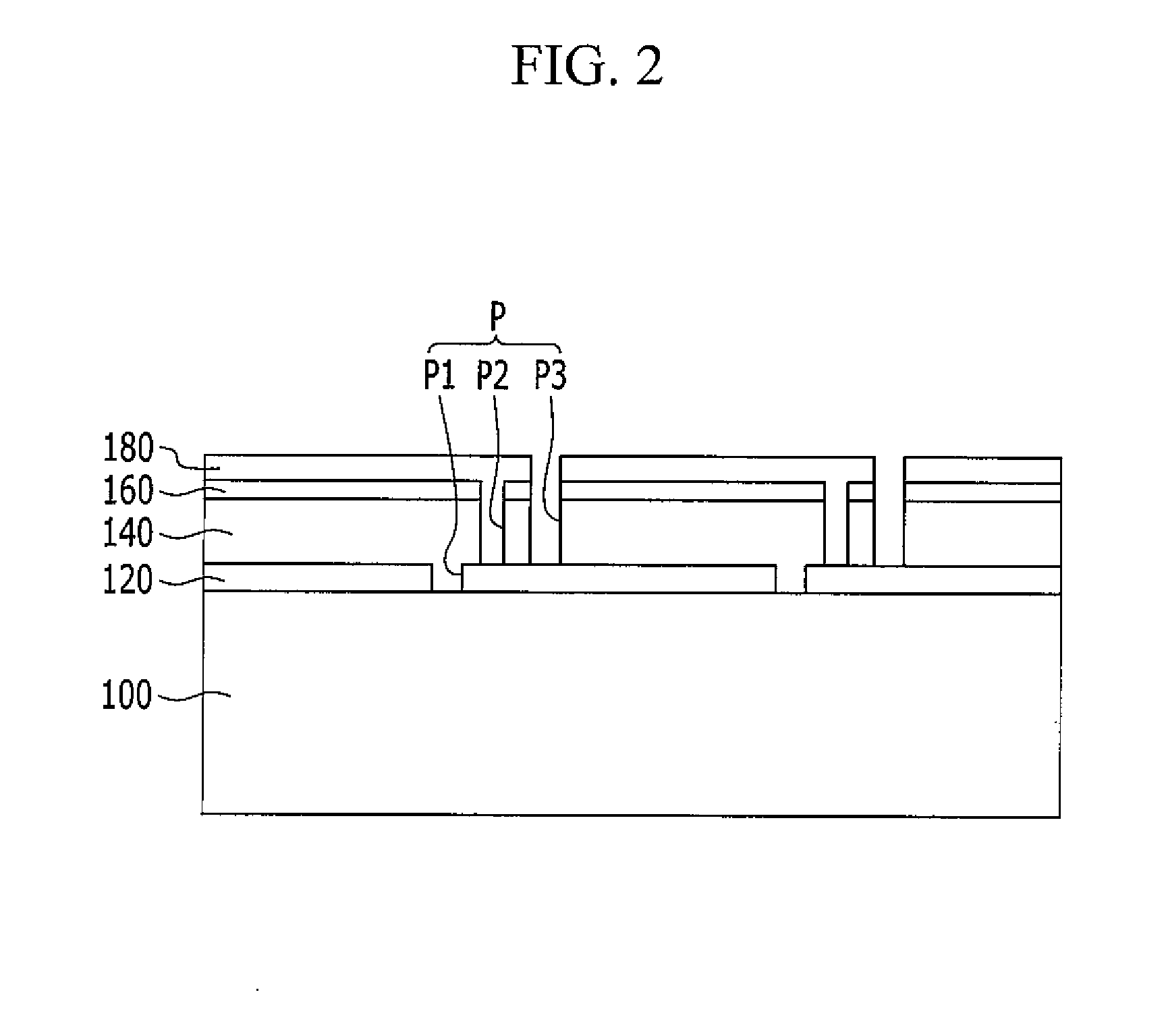
Figure 3
Abstract
Description
CROSS-REFERENCE TO RELATED APPLICATION
[0001] This application claims priority to and the benefit of Korean Patent Application No. 10-2013-0141705 filed in the Korean Intellectual Property Office on Nov. 20, 2013, the entire contents of which are incorporated herein by reference.BACKGROUND
[0002] 1. Field
[0003] The described technology relates generally to a solar cell.
[0004] 2. Description of the Related Art
[0005] A solar cell, which is a photovoltaic device that converts solar energy into electrical energy, is a next-generation pollution free energy source.
[0006] A solar cell typically includes p-type semiconductor and n-type semiconductor. When solar energy is absorbed at an optical active layer, an electron-hole pair (EHP) is generated in the semiconductor, wherein the generated electron and hole move to the n-type semiconductor and the p-type semiconductor, respectively, and are collected by electrodes, electrical energy can be generated.
[0007] As the optical active layer, a compound se...
Examples
Embodiment Construction
[0047]Hereinafter, exemplary embodiments so as to be easily practiced by a person skilled in the art to which the present invention pertains will be described in detail with reference to the accompanying drawings. However, the present invention may be modified in various different ways and is not limited to the embodiments provided in the present description.
[0048]In the drawings, the thickness of layers, films, panels, regions, etc., are exaggerated for clarity. Like reference numerals designate like elements throughout the specification. It will be understood that when an element such as a layer, film, region, or substrate is referred to as being “on” another element, it can be directly on the other element or intervening elements may also be present. In contrast, when an element is referred to as being “directly on” another element, there are no intervening elements present.
[0049]Hereinafter, a solar cell will be described in detail with reference to the accompanying drawings.
[00...