
Psuedo resistor circuit and charge amplifier
a resistor circuit and charge amplifier technology, applied in the field of pseudo resistor circuits and charge amplifiers, can solve the problems of strong resistors and waveform distortion in signal output, and achieve the effects of reducing temperature dependence, reducing temperature dependence, and reducing waveform distortion caused by non-linearity of pseudo resistance values
Patent Information
- Authority / Receiving Office
- US · United States
- Patent Type
- Applications(United States)
- Current Assignee / Owner
- Publication Date
- 2016-01-21
Smart Images
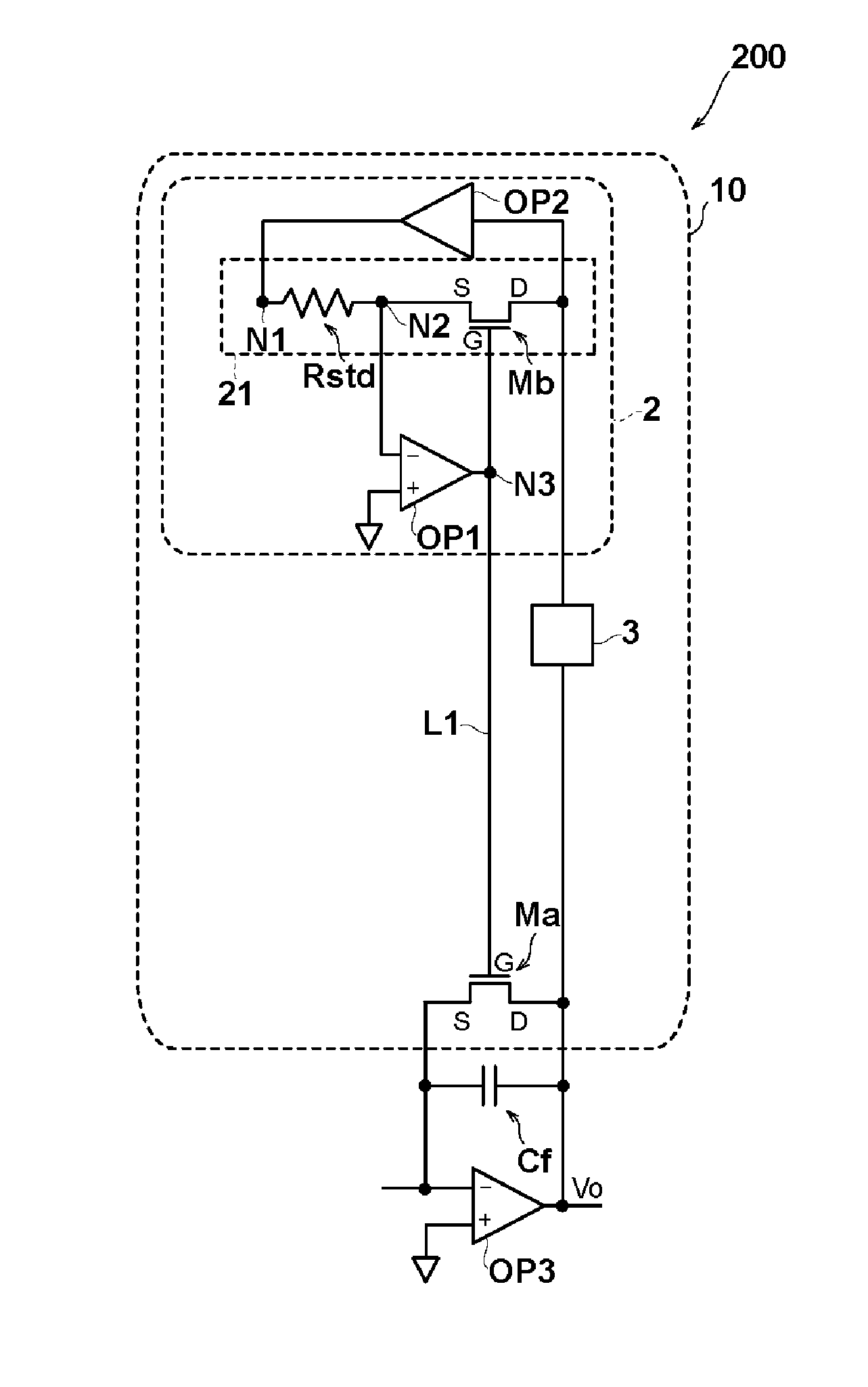
Figure 1 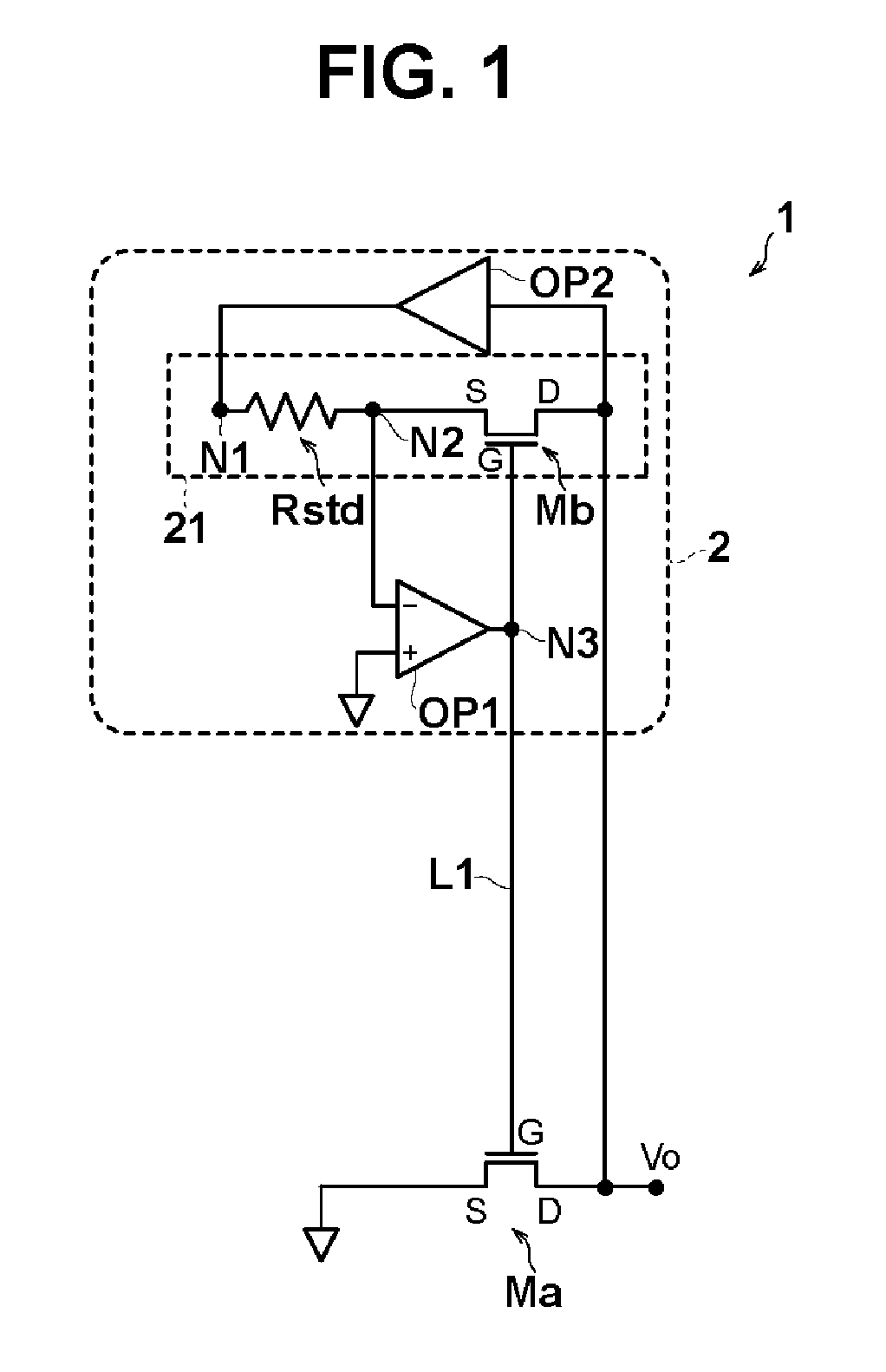
Figure 2 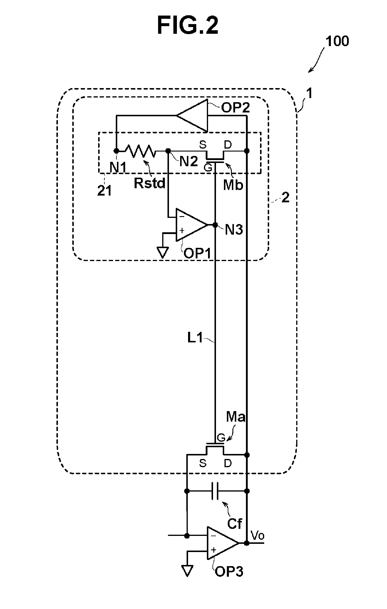
Figure 3
Abstract
Description
CROSS REFERENCE TO RELATED APPLICATIONS
[0001] The present application is a continuation of PCT / JP2014 / 058550 filed Mar. 26, 2014, which claims priority to Japanese Patent Application No. 2013-076986, filed Apr. 2, 2013, the entire contents of each of which are incorporated herein by reference.FIELD OF THE INVENTION
[0002] The present invention relates to pseudo resistor circuits and charge amplifiers. In particular, the present invention relates to a pseudo resistor circuit including a metal oxide semiconductor field effect transistor (MOSFET) used in a weak inversion region and a charge amplifier using the pseudo resistor circuit.BACKGROUND OF THE INVENTION
[0003] Charge output sensors have been in widespread use in recent years. The charge output sensors are electric charge generating sensors, such as strain gauges and acceleration sensors, using piezoelectric elements made of insulating material. Since minor electric charge is detected in such a charge output sensor, it is necessary t...
Examples
first embodiment
[0060]First, a pseudo resistor circuit in a first embodiment of the present invention and a charge amplifier using the pseudo resistor circuit will be described in detail with reference to FIG. 1 and FIG. 2.
[0061]FIG. 1 is a circuit diagram illustrating a configuration of the pseudo resistor circuit in the present embodiment. FIG. 2 is a circuit diagram illustrating a configuration of the charge amplifier to which the pseudo resistor circuit in the present embodiment is applied.
[0062][Configuration of Pseudo Resistor Circuit]
[0063]The configuration of a pseudo resistor circuit 1 in the present embodiment will be described in detail with reference to FIG. 1.
[0064]As illustrated in FIG. 1, the pseudo resistor circuit 1 in the present embodiment includes a first field effect transistor Ma and a distortion compensation bias source 2 that reduces waveform distortion caused by a variation in resistance value of the first field effect transistor Ma.
[0065]The first field effect transistor M...
second embodiment
[0089]Next, a pseudo resistor circuit in a second embodiment of the present invention and a charge amplifier using the pseudo resistor circuit will be described in detail with reference to FIG. 3 and FIG. 4.
[0090]FIG. 3 is a circuit diagram illustrating a configuration of the pseudo resistor circuit in the present embodiment. FIG. 4 is a circuit diagram illustrating a configuration of the charge amplifier to which the pseudo resistor circuit in the present embodiment is applied.
[0091]As illustrated in FIG. 3 and FIG. 4, a pseudo resistor circuit 10 in the present embodiment and a charge amplifier 200 using the pseudo resistor circuit 10 mainly differ from the pseudo resistor circuit 1 in the first embodiment and the charge amplifier 100 using the pseudo resistor circuit 1 in that an absolute value circuit 3 is added. The remaining configurations of the pseudo resistor circuit 10 and the charge amplifier 200 are the same as those of the pseudo resistor circuit 1 and the charge amplif...
third embodiment
[0105]Next, a pseudo resistor circuit in a third embodiment of the present invention and a charge amplifier using the pseudo resistor circuit will be described in detail with reference to FIG. 5 and FIG. 6.
[0106]FIG. 5 is a circuit diagram illustrating a configuration of the pseudo resistor circuit in the present embodiment. FIG. 6 is a circuit diagram illustrating a configuration of the charge amplifier to which the pseudo resistor circuit in the present embodiment is applied.
[0107]As illustrated in FIG. 5 and FIG. 6, a pseudo resistor circuit 20 in the present embodiment and a charge amplifier 300 using the pseudo resistor circuit 20 mainly differ from the pseudo resistor circuit 10 in the second embodiment and the charge amplifier 200 using the pseudo resistor circuit 10 in that a direct-current voltage source 4 is added. The remaining configurations of the pseudo resistor circuit 20 and the charge amplifier 300 are the same as those of the pseudo resistor circuit 10 and the char...