
Assembly method and plant of photovoltaic panel of the back-contact type, with printing on the cells combined with loading and pre-fixing
a photovoltaic panel and back contact technology, applied in the direction of semiconductor/solid-state device manufacturing, electrical apparatus, semiconductor devices, etc., can solve the problems of high precision, high risk of flashing or incomplete laying, and difficulty in handling and aligning a large printing screen on all the contacting points of the conductive backsheet. , to achieve the effect of facilitating the picking up of single cells
Patent Information
- Authority / Receiving Office
- US · United States
- Current Assignee / Owner
- Publication Date
- 2021-03-25
Smart Images
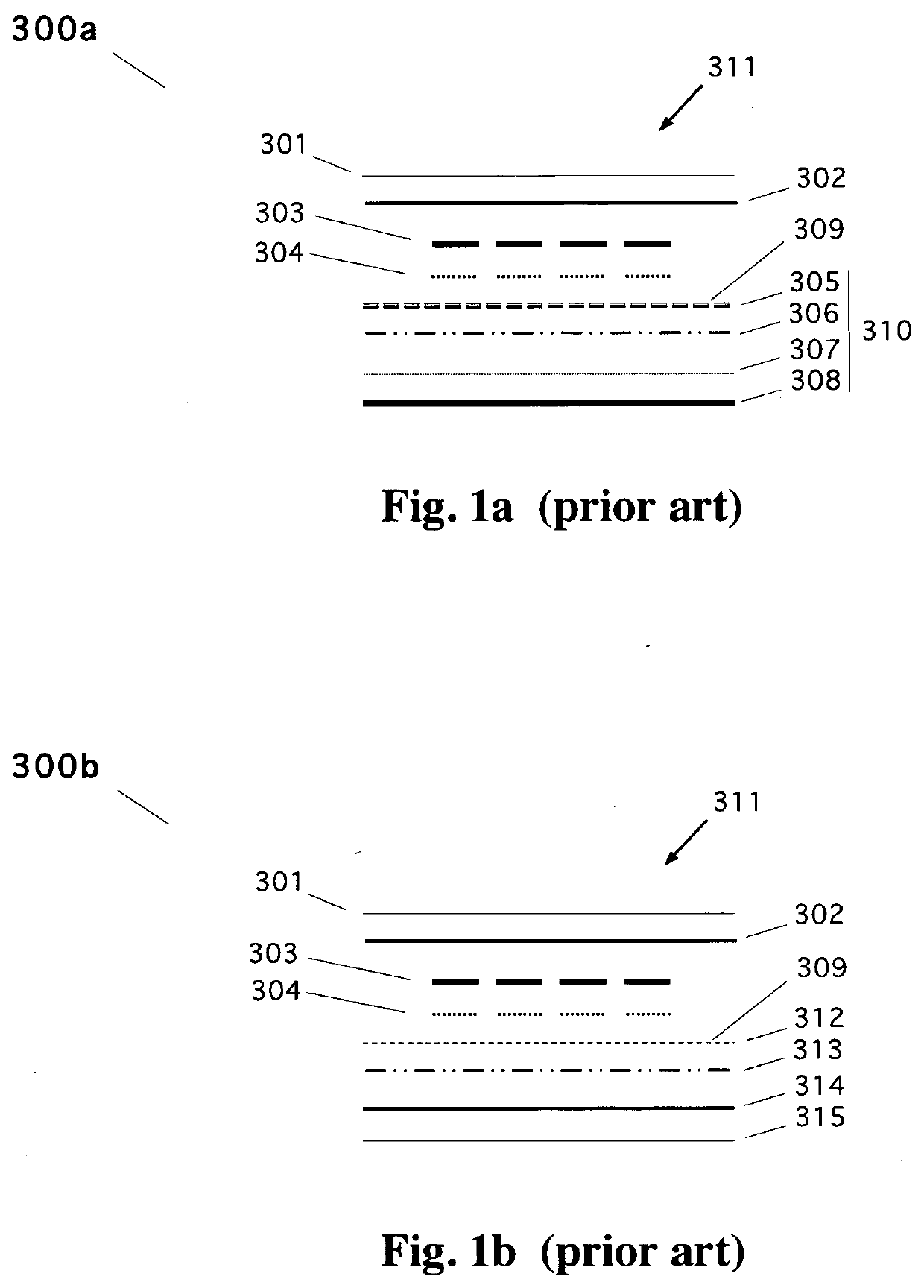
Figure 1 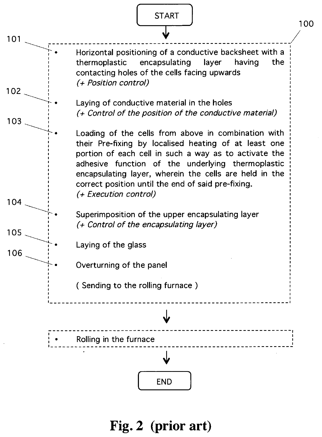
Figure 2 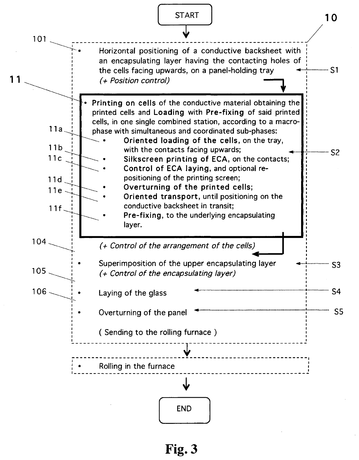
Figure 3
Abstract
Description
[0001] The present invention relates to an assembly method of a photovoltaic panel with back-contact solar cells of crystalline silicon, with printing on the cells combined with loading and pre-fixing of the printed cells on a conductive backsheet. In particular, the proposed method provides a multiple operating phase called macro-phase in which, in a simultaneous and coordinated way, the cell is picked up and conductive adhesive ECA is printed on the contacts facing upwards, and a string of printed cells is immediately overturned and positioned on the conductive backsheet in transit, pre-fixing it in its final position. The present invention also relates to an advantageous automatic assembly plant comprising a combined station intended for the execution of said macro-phase.FIELD OF THE INVENTION
[0002] The invention finds particular application in the industrial sector of production of photovoltaic panels, with specific reference to the modern photovoltaic panels with back-contact cel...
Examples
Embodiment Construction
[0059]With reference to the figures (FIGS. 3, 4a, 4b, 5a, 5b, 6a, 6b) as well, an advantageous assembly method (10) with the related production equipment is described, that is to say, an automatic plant (20) which comprises a particular combined workstation (S2), for photovoltaic panels (300) with back-contact solar cells (303) of crystalline silicon. The invention provides a progressive layering of the components on a mobile tray starting from the back of the panel, that is to say, with the front glass facing upwards, wherein in said workstation (S2) said ECA conductive adhesive (304) is printed on the contacts of the cells (303) obtaining printed cells, and said printed cells are simultaneously loaded and pre-fixed on a particular conductive backsheet, called BCBS (310), which is already provided with the lower encapsulating layer with dielectric material and contacting holes.
[0060]The present invention provides great versatility of use, it being particularly suitable for panels o...