
Semiconductor structure and method for forming the same
Patent Information
- Authority / Receiving Office
- US · United States
- Current Assignee / Owner
- Publication Date
- 2022-01-27
Smart Images
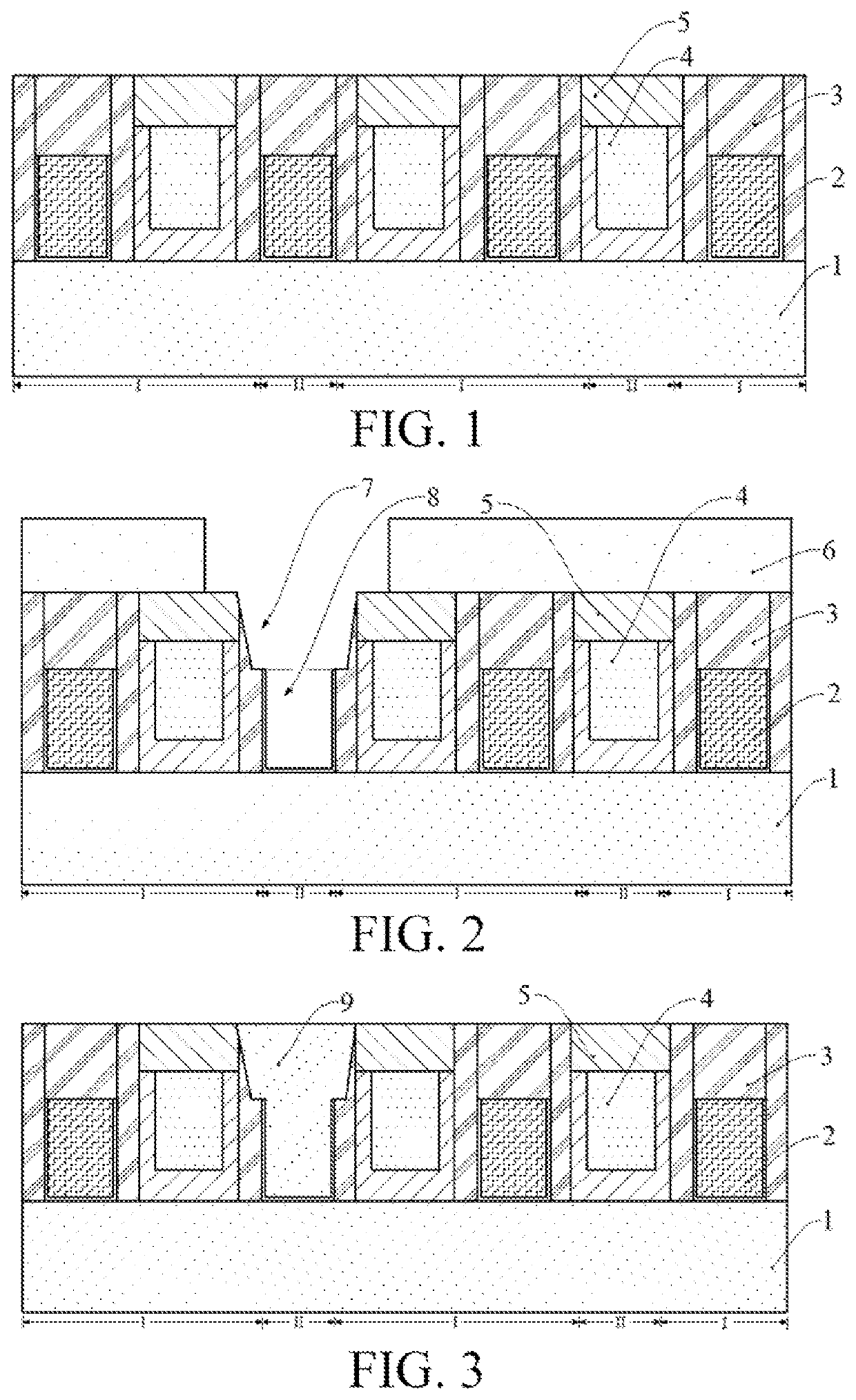
Figure 1 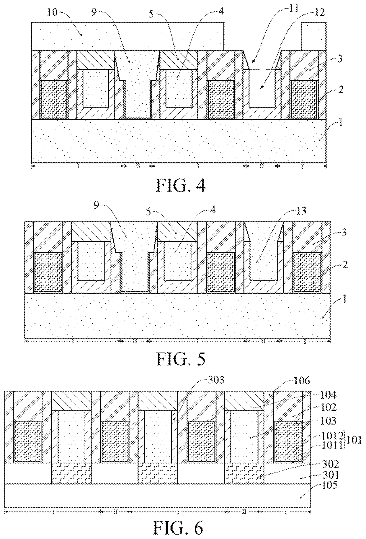
Figure 2 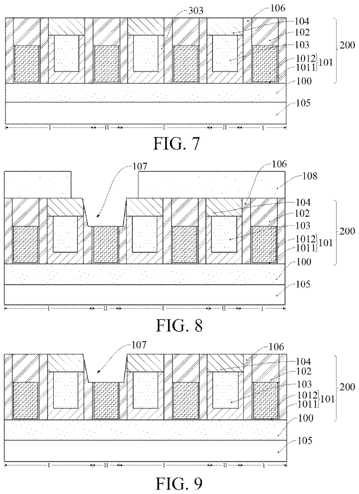
Figure 3
Abstract
Description
RELATED APPLICATIONS
[0001] The present application claims priority to Chinese Patent Appln. No. 202010725785.4, filed Jul. 24, 2020, the entire disclosure of which is hereby incorporated by reference.BACKGROUNDTechnical Field
[0002] Embodiments and implementations of the present disclosure relate to the field of semiconductor manufacturing, and in particular, to a semiconductor structure and a method for forming the same.Related Art
[0003] With the continuous development of integrated circuit manufacturing technologies, people have increasingly high requirements on the integration level and performance of integrated circuits. To improve the integration level and reduce costs, critical dimensions of the components are continuously reduced, and the circuit density inside the integrated circuit is becoming increasingly high. Such a development trend makes the wafer surface unable to provide a sufficient area for fabricating required interconnection lines.
[0004] To meet the requirement of the...
Examples
Embodiment Construction
[0030]As will be appreciated from the background, currently, formed device still have poor performance problems. Reasons for the poor performance of the devices are analyzed now in combination with a method for forming a semiconductor structure.
[0031]FIG. 1 to FIG. 5 are schematic structural diagrams corresponding to all steps in a method for forming a semiconductor structure.
[0032]As shown in FIG. 1, a base is provided. The base includes a device region I and a dummy device region II. The base includes an isolation layer 1, gate structures 2 located on the isolation layer 1, a first mask layer 3 located on the gate structures 2, a source-drain plug 4 located between the gate structures 2 and on the isolation layer 1, and a second mask layer 5 located on the source-drain plug 4.
[0033]As shown in FIG. 2, a first shielding layer 6 exposing the first mask layer 3 in the dummy device region II is formed. The first mask layer 3 on the gate structures 2 of the dummy device region II is re...