
Flash memory device and erase method using the same
a flash memory and erase technology, applied in static storage, digital storage, instruments, etc., can solve the problem of rising the voltage of the word line of an unselected cell block, and achieve the effect of shortening the erase time of the devi
Patent Information
- Authority / Receiving Office
- US · United States
- Patent Type
- Patents(United States)
- Current Assignee / Owner
- Publication Date
- 2010-07-20
Smart Images
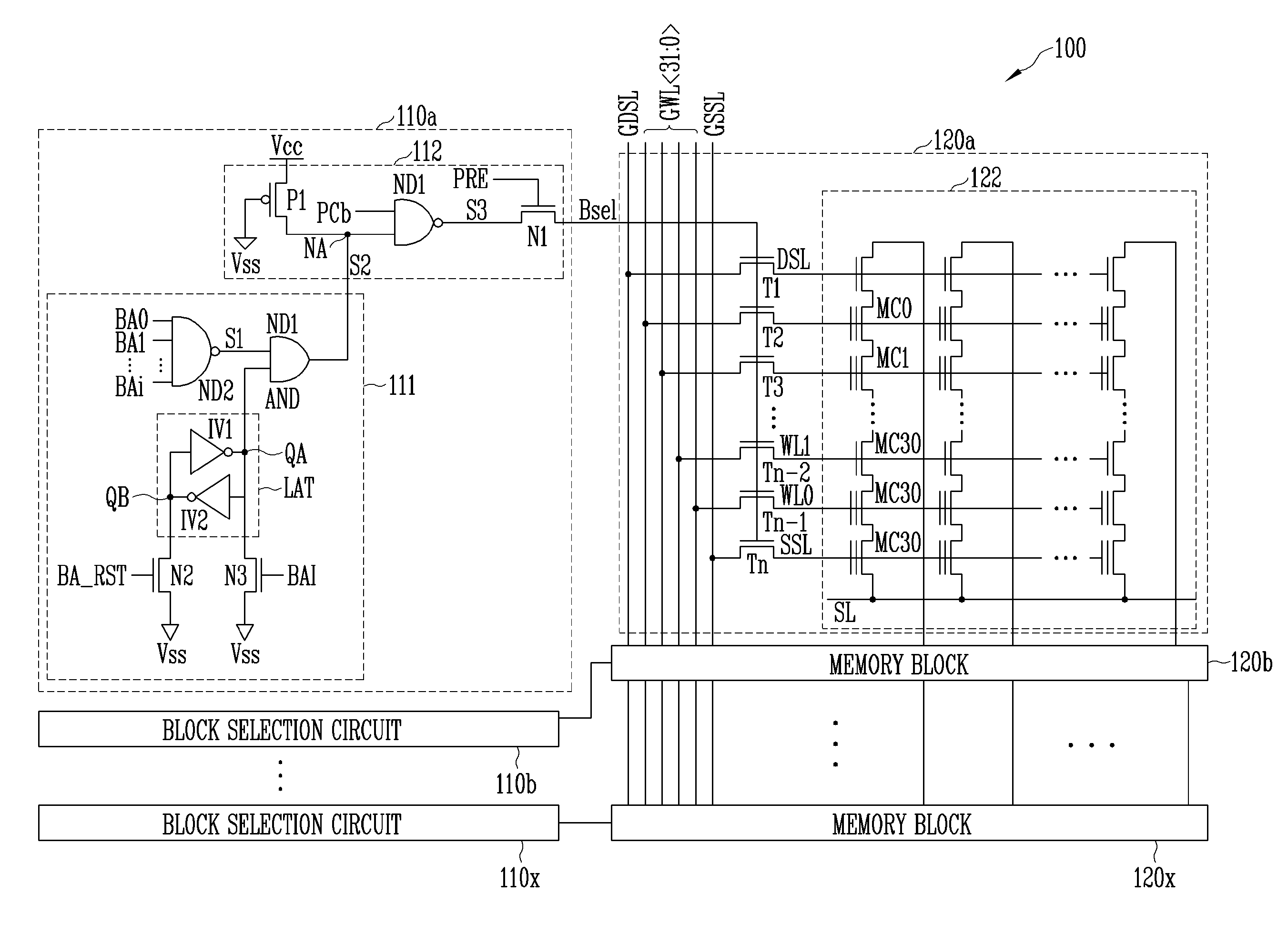
Figure 1 
Figure 2 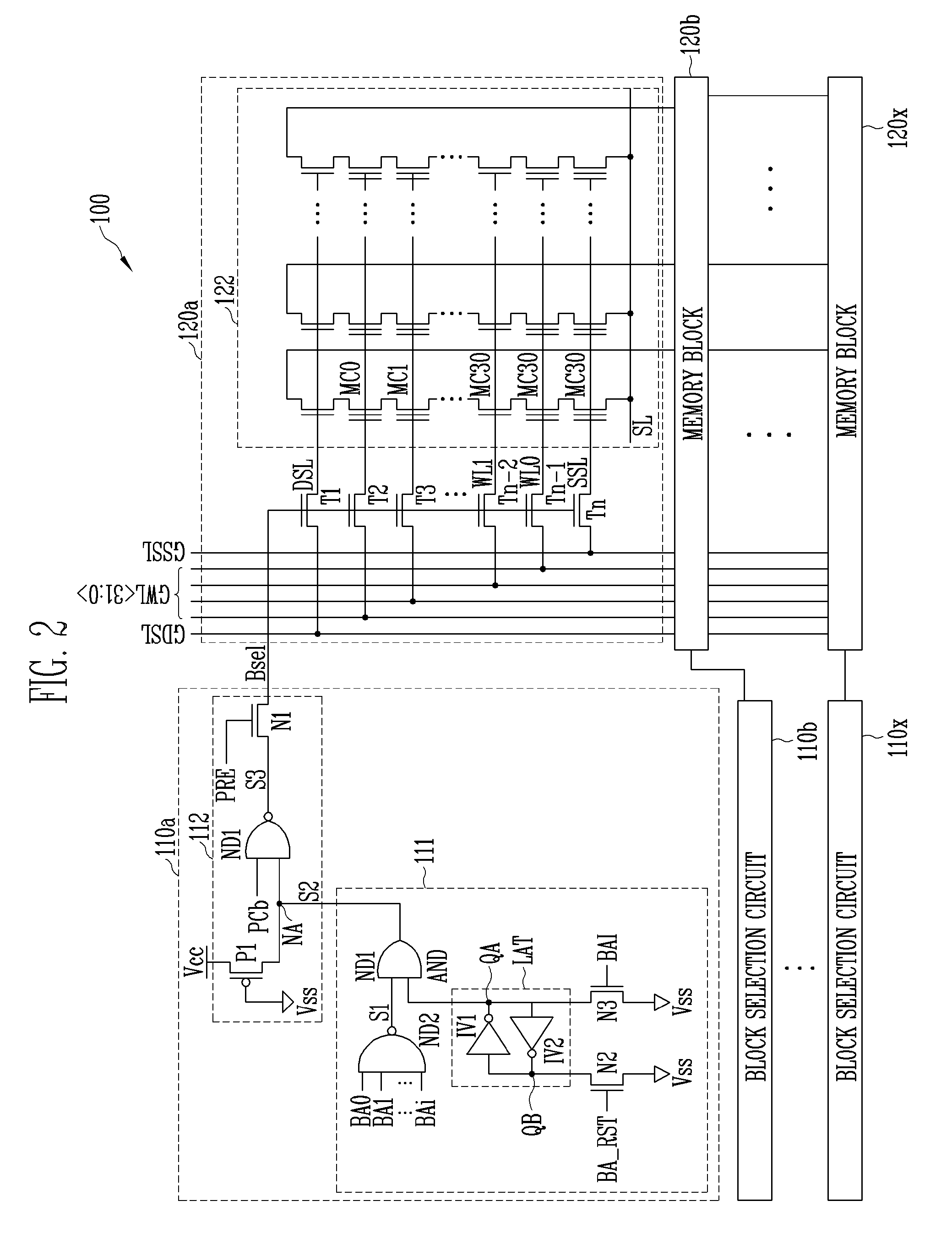
Figure 3
Abstract
Description
CROSS-REFERENCES TO RELATED APPLICATIONS
[0001] The present application claims priority to Korean patent application number 10-2006-96186, filed on Sep. 29, 2006, which is incorporated by reference in its entirety.BACKGROUND OF THE INVENTION
[0002] The present invention relates, in general, to flash memory devices and, more particularly, to a flash memory device and an erase method using the same, in which a plurality of blocks are erased at the same time, shortening an erase time.
[0003] In general, a NAND flash memory device includes a plurality of cell blocks. One cell block includes a plurality of cell strings in which a plurality of cells are connected in series, a plurality of bit lines, a plurality of word lines, a drain select transistor connected between the cell strings and the bit lines, and a source select transistor connected between the cell strings and a common source line.
[0004] Meanwhile, the plurality of memory cells sharing one word line constitutes one page. The entire ...
Examples
Embodiment Construction
[0017]Embodiments according to the present invention will be described with reference to the accompanying drawings.
[0018]FIG. 2 is a circuit diagram of a flash memory device including a block switch circuit according to an embodiment of the present invention.
[0019]Referring to FIG. 2, a flash memory device 100 includes a plurality of block selection circuits 110a to 110x (where “a” to “x” are positive integers), and a plurality of memory blocks 120a to 120x (where “a” to “x” are positive integers). The plurality of block selection circuits 110a to 110x are connected to the plurality of memory blocks 120a to 120x, respectively.
[0020]The plurality of block selection circuits 110a to 110x have similar construction and operations. Thus, only the block selection circuit 110a is described as an example.
[0021]The block selection circuit 110a includes a control signal generator 111 and a select signal generator 112.
[0022]The control signal generator 111 generates a select control signal S2 ...