
Flash memory device with reduced erase time
a flash memory and erase time technology, applied in static storage, digital storage, instruments, etc., can solve the problems of increasing the complexity of the reality, affecting the efficiency of flash memory devices, and eprom devices having a limited lifetime, so as to reduce the erase time
Patent Information
- Authority / Receiving Office
- US · United States
- Patent Type
- Patents(United States)
- Current Assignee / Owner
- Publication Date
- 2008-05-13
Smart Images
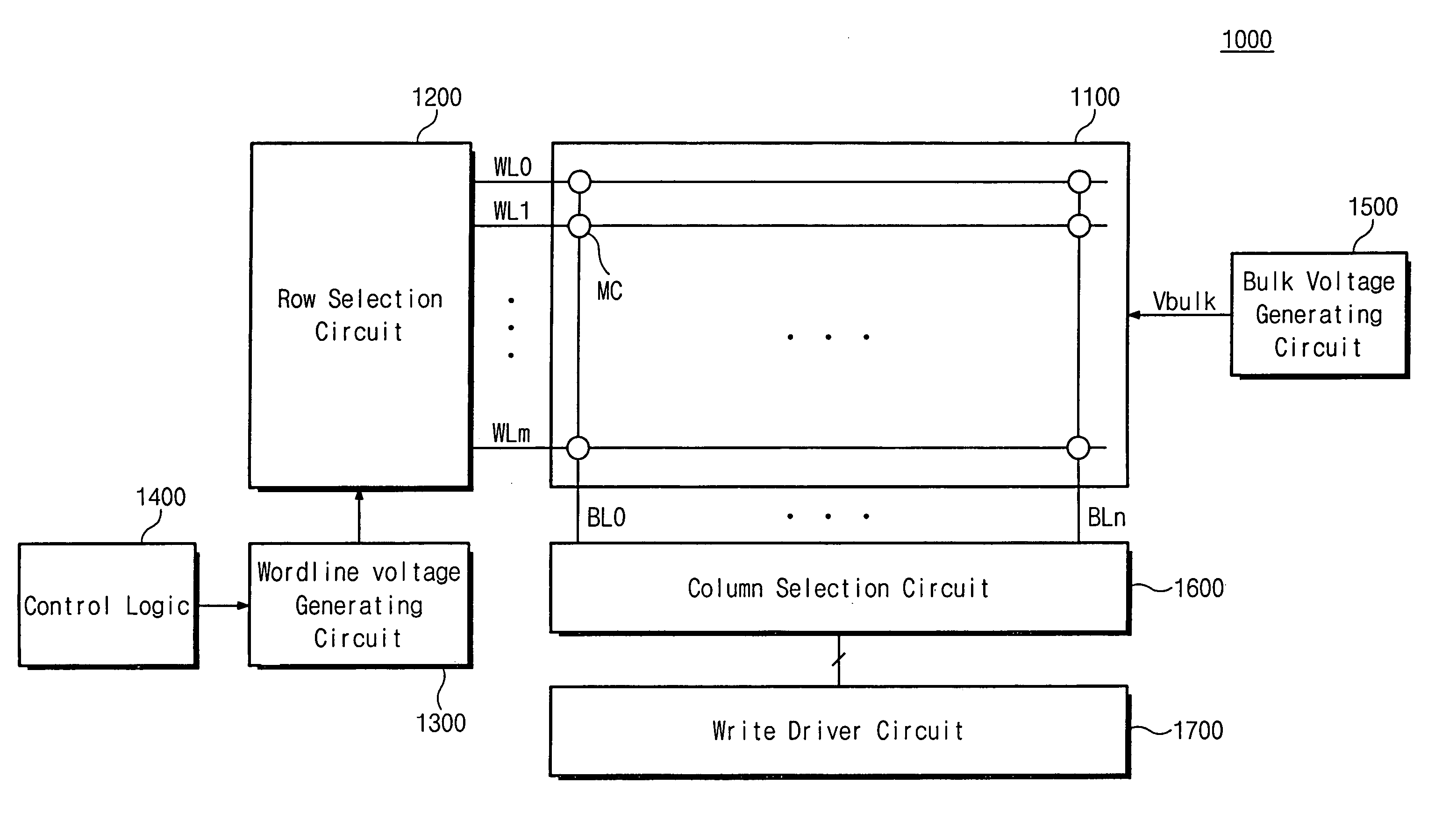
Figure 1 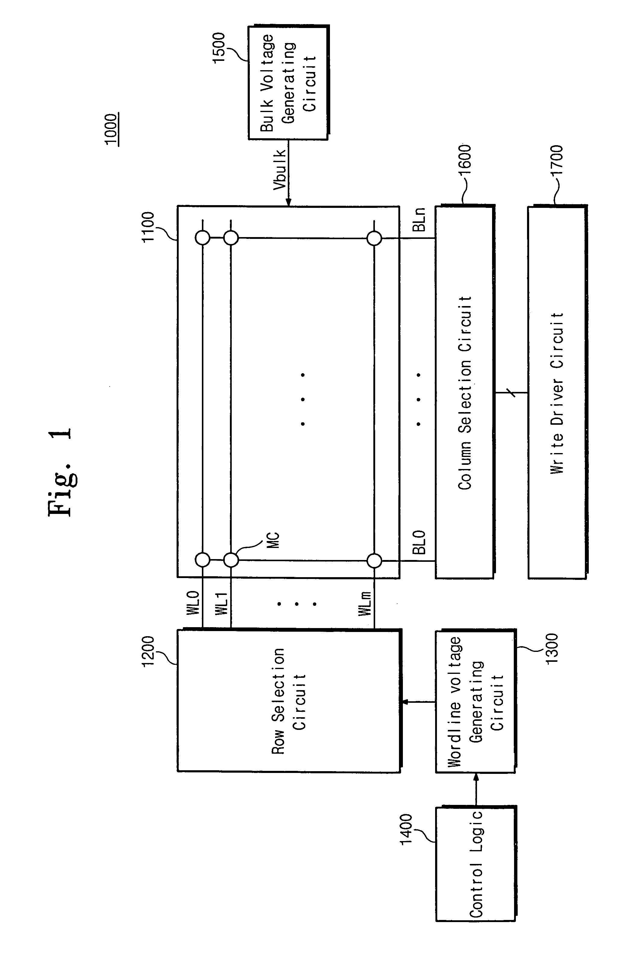
Figure 2 
Figure 3
Abstract
Description
BACKGROUND OF THE INVENTION
[0001] 1. Field of the Invention
[0002] Embodiments of the present invention are related to semiconductor memory devices. In particular, embodiments of the invention are related to flash memory devices.
[0003] This application claims priority to Korean Patent Application No. 2005-80164, filed Aug. 30, 2005, the subject matter of which is hereby incorporated by reference in its entirety.
[0004] 2. Description of Related Art
[0005] Flash memory is one type of non-volatile memory. It is commonly used as a replacement for conventional electrically erasable programmable read only memory (EEPROM) which is generally formed by plural memory sectors, each being erasable and / or programmable using a single programming operation. Thus, while conventional EEPROM devices are well adapted to slow speed applications which do not suffer from the fact that erase and programming operations must be carried on a memory block by memory block basis, flash memory devices are efficiently a...
Examples
Embodiment Construction
[0029]FIG. 1 is a block diagram showing an exemplary flash memory device in accordance to one embodiment of the invention.
[0030]Referring to FIG. 1, a NOR flash memory device 1000 comprises a memory cell array 1100 adapted to store information in the form of data values. Memory cell array 1100 comprises non-volatile memory cells (MC) disposed at the respective intersections of wordlines WL0˜WLm (or rows) and bitlines BL0˜BLn (or columns). Each memory cell MC may be adapted to store either 1-bit data or 2-bit data. A row selection circuit 1200 drives the wordlines WL0˜WLm with an erase voltage provided by a wordline voltage generating circuit 1300 during erase operations. Row selection circuit 1200 selects one wordline during program / read operations and drives the selected wordline with a program / read voltage provided by wordline voltage generating circuit 1300. Wordline voltage generating circuit 1300 is controlled by a control logic 1400 and appropriately constructed (as convention...