
Method for fabricating memory device
Patent Information
- Authority / Receiving Office
- US · United States
- Current Assignee / Owner
- Publication Date
- 2015-06-30
Smart Images
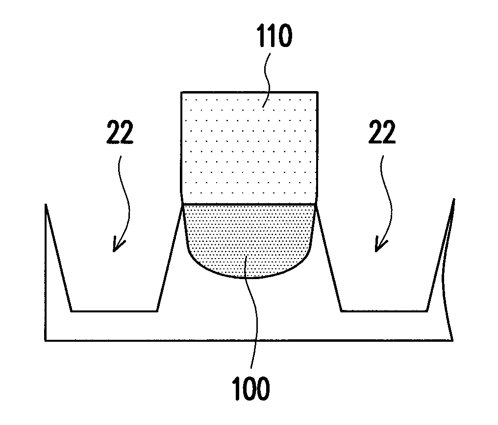
Figure 1 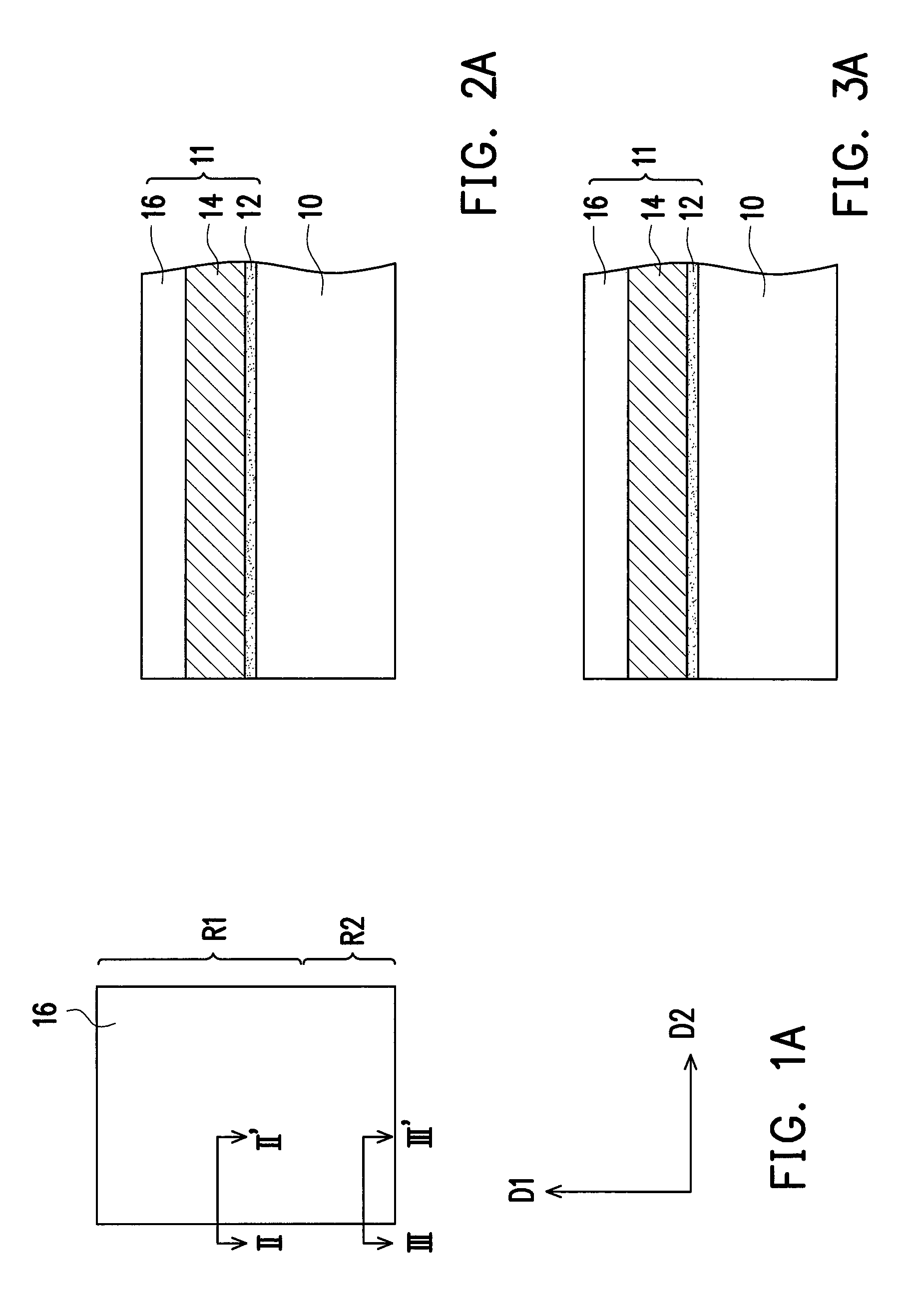
Figure 2 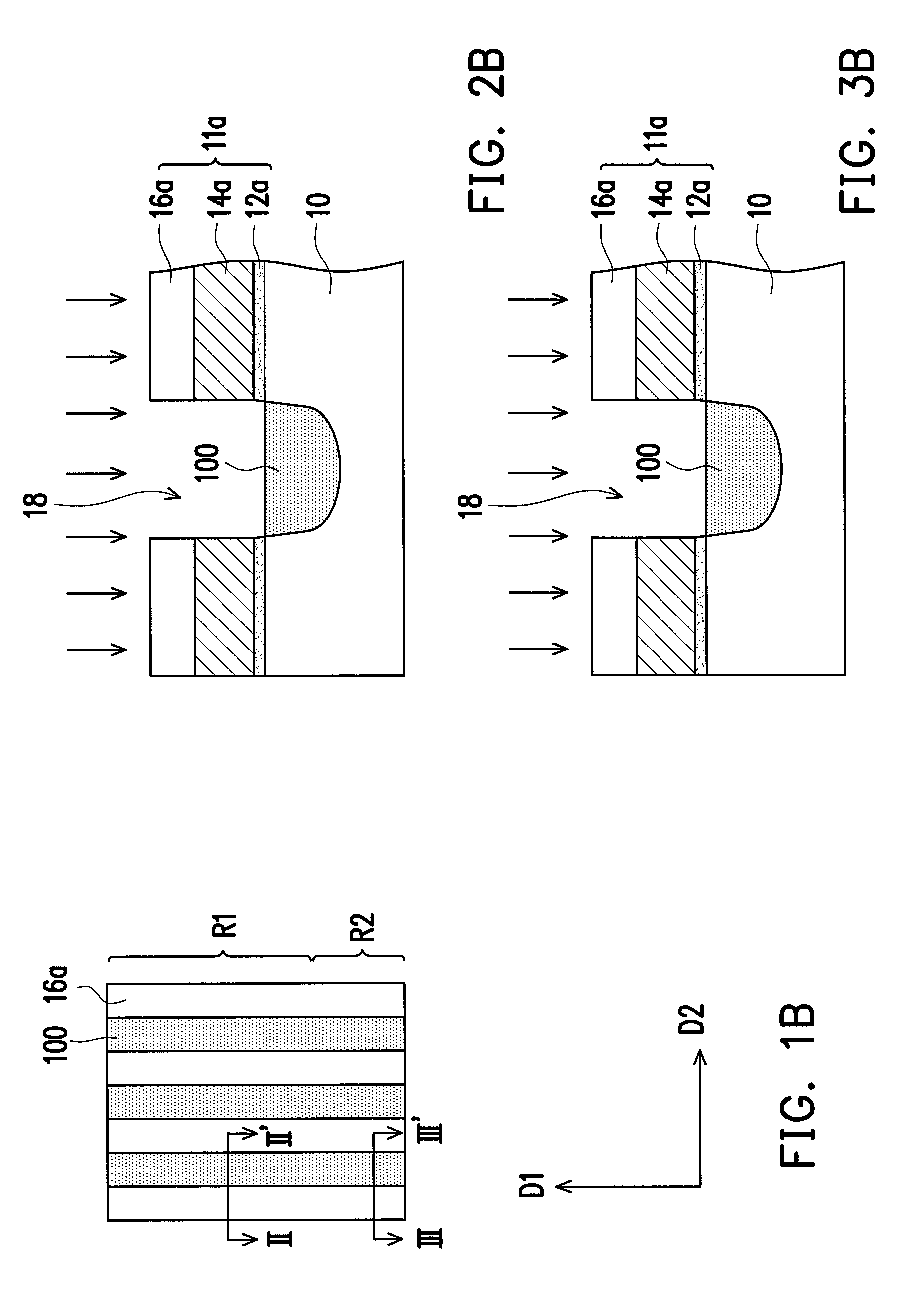
Figure 3
Abstract
Description
BACKGROUND OF THE INVENTION
[0001] 1. Field of the Invention
[0002] The invention relates to a method for fabricating a semiconductor device, and particularly relates to a method for fabricating a memory device.
[0003] 2. Description of Related Art
[0004] Memory may be categorized into volatile memory and non-volatile memory. When power supply is shut down, data stored in volatile memory disappears. However, non-volatile memory is characterized by maintaining the stored data even when the power is shut down. After the power supply is restored, the data stored in the memory may be read. Thus, non-volatile memory is generally applicable to electronic products, such as portable products.
[0005] As the integrity of memory devices increases and the size thereof is reduced, a plurality of isolation structures and dielectric layers are necessary to be formed to ensure that a plurality of memory cells are electrically insulated from each other. However, the plurality of isolation structures and diele...
Examples
Embodiment Construction
[0031]FIGS. 1A to 1K are top views illustrating a flow for fabricating a memory device according to an embodiment of the invention. FIGS. 2A to 2K are respectively cross-sectional schematic views taken along a II-II′ line in FIGS. 1A to 1K. FIGS. 3A to 3K are respectively cross-sectional schematic views taken along a III-III′ line in FIGS. 1A to 1K. FIG. 4 is a cross-sectional schematic view taken along a IV-IV′ line in FIG. 1K.
[0032]Referring to FIGS. 1A, 2A, and 3A, first of all, a stack layer 11 is formed on a substrate 10. The substrate 10 has a first region R1 and a second region R2, as shown in FIG. 1A. In an embodiment of the invention, the first region R1 may be an active region, for example, while the second region R2 may be a peripheral region, for example. The substrate 10 is a semiconductor substrate, a semiconductor compound substrate, or a semiconductor-over-insulator (SOI) substrate. The semiconductor is, for example, atoms in group IVA, such as silicon or germanium. ...