Analysis of Flexible Microdisplay Emission Technology
OCT 21, 20259 MIN READ
Generate Your Research Report Instantly with AI Agent
Patsnap Eureka helps you evaluate technical feasibility & market potential.
Flexible Microdisplay Technology Evolution and Objectives
Flexible microdisplay technology has evolved significantly over the past two decades, transitioning from rigid display structures to increasingly flexible and adaptable solutions. The journey began with early experiments in flexible substrates during the early 2000s, primarily focused on e-paper displays with limited functionality and resolution. These initial developments laid the groundwork for more sophisticated approaches that would follow.
By the mid-2010s, OLED (Organic Light-Emitting Diode) technology emerged as a pivotal advancement, enabling thinner, lighter, and more flexible display configurations. This period marked a critical shift from theoretical research to practical applications, with several major electronics manufacturers demonstrating prototype flexible displays at industry exhibitions. The evolution accelerated with the introduction of plastic substrates replacing traditional glass components, significantly enhancing flexibility while maintaining optical performance.
Recent technological breakthroughs have centered on addressing key challenges in flexible emission technology, particularly the development of robust thin-film transistor (TFT) backplanes that can withstand repeated bending without performance degradation. Innovations in materials science have produced new semiconductor compounds and electrode materials specifically engineered for flexibility, durability, and efficient light emission under mechanical stress conditions.
The current trajectory of flexible microdisplay technology is moving toward ultra-thin form factors with thickness below 10 micrometers, enabling conformable displays that can adapt to various surface geometries. Simultaneously, researchers are pursuing higher resolution capabilities, with pixel densities exceeding 1000 PPI (pixels per inch) for applications in near-eye displays and augmented reality systems.
The primary technical objectives in this field include achieving full-color gamut representation with high brightness uniformity across bent surfaces, minimizing power consumption for mobile applications, and extending operational lifetime under repeated mechanical deformation. Additionally, there is significant focus on developing manufacturing processes that can scale efficiently while maintaining precise tolerances required for microdisplay production.
Looking forward, the industry aims to integrate flexible microdisplays with other emerging technologies such as stretchable electronics and self-healing materials to create truly conformable visual interfaces. The ultimate goal encompasses creating display systems that can seamlessly blend with various environments and form factors while delivering high-quality visual information, potentially revolutionizing fields ranging from consumer electronics to medical imaging and automotive displays.
Market Demand Analysis for Flexible Display Solutions
The flexible microdisplay market has witnessed substantial growth in recent years, driven by increasing consumer demand for wearable devices, augmented reality (AR), virtual reality (VR), and foldable smartphones. According to industry reports, the global flexible display market reached approximately $23 billion in 2022 and is projected to grow at a compound annual growth rate of 35% through 2028, with microdisplays representing a significant segment within this market.
Consumer electronics remains the primary driver for flexible microdisplay technology adoption. The wearable device segment, including smartwatches and fitness trackers, has shown particular affinity for flexible displays due to their ability to conform to the human body's contours. Market research indicates that shipments of wearable devices incorporating flexible display technology increased by 27% year-over-year in 2022, demonstrating strong consumer acceptance.
The AR/VR sector presents perhaps the most promising growth opportunity for flexible microdisplay technology. As these immersive technologies transition from niche applications to mainstream consumer products, demand for lightweight, energy-efficient, and high-resolution flexible displays has intensified. Industry analysts predict that AR headset shipments will grow from 3.5 million units in 2022 to over 28 million units by 2026, creating substantial demand for advanced flexible microdisplay solutions.
Healthcare applications represent an emerging market segment with significant potential. Medical professionals are increasingly utilizing AR headsets with flexible microdisplays for surgical planning, medical training, and patient care. The healthcare AR market is expected to grow at 38% annually through 2027, creating new opportunities for specialized flexible display technologies that meet medical-grade requirements.
Automotive applications are also driving demand for flexible microdisplay technology. Heads-up displays (HUDs) and advanced driver assistance systems (ADAS) increasingly incorporate flexible display components to provide drivers with critical information while maintaining visibility of the road. The automotive display market is projected to reach $30 billion by 2025, with flexible technologies capturing an increasing share.
Regional analysis reveals that Asia-Pacific dominates the flexible display manufacturing landscape, with South Korea, Japan, and China leading production capacity. However, North America represents the largest market for end-use applications, particularly in AR/VR and medical sectors, while Europe shows strong demand in automotive applications.
Key market challenges include production costs, yield rates, and durability concerns. Despite these challenges, consumer willingness to pay premium prices for devices with flexible display technology remains strong, with surveys indicating that 65% of smartphone users would consider paying more for foldable devices with advanced display capabilities.
Current Emission Technology Landscape and Challenges
The flexible microdisplay emission technology landscape is currently dominated by several key technologies, each with distinct advantages and limitations. OLED (Organic Light-Emitting Diode) technology leads the market due to its inherent flexibility, self-emissive properties, and excellent color reproduction. However, OLED displays face persistent challenges including limited lifetime, particularly for blue emitters, and susceptibility to moisture and oxygen degradation, necessitating complex encapsulation solutions for flexible applications.
Micro-LED technology represents a promising alternative, offering superior brightness, energy efficiency, and longevity compared to OLEDs. Despite these advantages, the mass transfer of microscopic LED chips onto flexible substrates remains technically challenging and cost-prohibitive for widespread commercial adoption. Current yield rates in the transfer process significantly impact production economics, particularly for high-resolution displays.
Quantum Dot (QD) emission technologies are emerging as contenders in the flexible display market, with exceptional color purity and stability. QD-OLED hybrid approaches are gaining traction, though the integration of quantum dots into truly flexible form factors presents material science challenges related to maintaining quantum efficiency when subjected to mechanical stress.
The substrate technology underpinning flexible displays presents its own set of challenges. Polyimide films currently serve as the predominant substrate material, but issues with oxygen and moisture permeability continue to affect emission layer longevity. Alternative substrate materials such as ultrathin glass offer improved barrier properties but introduce trade-offs in terms of flexibility range and durability against repeated bending.
Thin-film encapsulation (TFE) technologies represent a critical component of the emission technology landscape, with atomic layer deposition (ALD) and organic-inorganic hybrid approaches competing to provide the optimal balance between barrier performance and mechanical flexibility. Current state-of-the-art TFE solutions still struggle to maintain perfect barrier properties under extreme bending conditions.
From a manufacturing perspective, the industry faces significant yield challenges in producing consistent emission characteristics across large flexible surfaces. Roll-to-roll processing shows promise for cost reduction but introduces additional variables affecting emission uniformity. The integration of driving circuits with flexible emission layers presents another hurdle, with various approaches including low-temperature polysilicon (LTPS) and oxide TFT technologies competing for dominance.
Geographically, South Korea and China lead in flexible OLED manufacturing capacity, while Taiwan maintains strength in TFT backplane technologies. European research institutions are advancing next-generation quantum dot materials, and North American companies focus on innovative micro-LED transfer techniques and advanced encapsulation solutions.
Current Emission Solutions for Flexible Microdisplays
01 Flexible OLED technology for microdisplays
Organic Light Emitting Diode (OLED) technology is utilized in flexible microdisplays due to its self-emissive properties and ability to be fabricated on flexible substrates. These displays can be bent or curved without losing functionality, making them suitable for wearable devices and curved display applications. The technology incorporates thin-film transistors on flexible substrates to control the emission of light from organic materials, resulting in lightweight and durable microdisplays with high contrast ratios and wide viewing angles.- Flexible OLED technology for microdisplays: Organic Light Emitting Diode (OLED) technology is utilized in flexible microdisplays due to its self-emissive properties and ability to be fabricated on flexible substrates. These displays can be bent or curved without losing functionality, making them ideal for wearable devices and portable electronics. The technology incorporates specialized emission layers and electrode configurations that maintain performance integrity even when flexed.
- Backplane architecture for flexible displays: Advanced backplane architectures are essential for flexible microdisplays, incorporating thin-film transistors (TFTs) on flexible substrates. These designs include specialized driving circuits that can withstand mechanical stress while maintaining stable emission characteristics. The backplane technology enables uniform current distribution across the display area even when the display is bent or deformed, ensuring consistent image quality.
- Optical systems for flexible microdisplays: Specialized optical systems are developed for flexible microdisplays to maintain image quality during deformation. These systems include adaptive lenses, light management films, and optical compensation layers that adjust to changes in display curvature. The optical components work together to minimize distortion and maintain brightness uniformity across the flexible emission surface, enhancing the viewing experience regardless of display configuration.
- Testing and quality control for flexible emission displays: Specialized testing methodologies and equipment are developed for evaluating the performance of flexible microdisplays under various bending conditions. These include automated optical inspection systems, electrical testing under mechanical stress, and accelerated aging tests specific to flexible display technologies. The testing procedures ensure that emission characteristics remain stable and uniform throughout the expected lifetime of the display, even after repeated flexing cycles.
- Integration technologies for flexible display systems: Advanced integration technologies enable the incorporation of flexible microdisplays into complete display systems. These include specialized interconnect solutions that maintain electrical connectivity during flexing, interface circuits that adapt to changing display geometries, and system-level designs that accommodate the unique requirements of flexible emission displays. The integration approaches focus on minimizing stress points while maximizing display area and functionality in compact form factors.
02 Backplane technology for flexible displays
Advanced backplane technologies are essential for flexible microdisplay emission systems. These include thin-film transistor arrays fabricated on flexible substrates that control pixel activation and emission intensity. Various semiconductor materials and manufacturing techniques are employed to create backplanes that maintain electrical performance while being mechanically flexible. The backplane design must accommodate bending stress while maintaining stable electrical characteristics to ensure consistent display performance across the entire flexible surface.Expand Specific Solutions03 Optical systems for flexible microdisplays
Specialized optical systems are developed for flexible microdisplay applications to maintain image quality despite the curved or flexible nature of the display surface. These systems include micro-lens arrays, waveguides, and optical films that help direct light emission, enhance brightness, and maintain viewing angles. The optical components must themselves be flexible or designed to accommodate the changing geometry of the display while preserving image quality and minimizing distortion when the display is flexed or bent.Expand Specific Solutions04 Driving methods for flexible emission displays
Unique driving methods are required for flexible microdisplay emission to ensure uniform brightness and color accuracy across curved surfaces. These methods include specialized timing controllers, voltage compensation algorithms, and current driving schemes that adjust for resistance variations caused by bending. Advanced driving techniques also address issues such as pixel non-uniformity and emission efficiency changes that occur when the display is flexed, ensuring consistent visual performance regardless of the display's physical configuration.Expand Specific Solutions05 Encapsulation and protection technologies
Specialized encapsulation and protection technologies are crucial for maintaining the longevity and performance of flexible microdisplay emission systems. These include thin-film encapsulation layers, moisture barriers, and protective coatings that shield the sensitive organic or inorganic emission materials from environmental factors while remaining flexible. Advanced multi-layer barrier films with alternating organic and inorganic layers provide effective protection against oxygen and moisture penetration while accommodating repeated bending and flexing without cracking or delamination.Expand Specific Solutions
Key Industry Players and Competitive Landscape
The flexible microdisplay emission technology market is currently in a growth phase, characterized by increasing demand for foldable and rollable displays across consumer electronics. The global market size is projected to reach significant value as major players invest heavily in R&D to overcome technical challenges in flexibility, durability, and mass production. Leading companies like Samsung Display, LG Display, and BOE Technology have achieved varying levels of technical maturity, with Samsung and LG demonstrating more advanced commercial implementations. Other significant competitors include TCL CSOT, Tianma Microelectronics, and E Ink, each focusing on different technological approaches from OLED to electrophoretic solutions. The competitive landscape shows Asian manufacturers dominating, with increasing collaboration between display manufacturers and semiconductor companies to advance integration capabilities.
LG Display Co., Ltd.
Technical Solution: LG Display has pioneered flexible microdisplay technology through their P-OLED (Plastic OLED) solution, which uses a plastic substrate instead of glass to achieve flexibility. Their technology incorporates a TFT backplane on polyimide film with OLED frontplane, enabling displays that can be bent, folded, and rolled. LG's proprietary WOLED (White OLED) technology employs a color filter approach where white light passes through RGB filters, simplifying manufacturing while maintaining high color accuracy. Their rollable OLED TV technology demonstrates the commercial viability of flexible displays at scale. LG has also developed ultra-thin glass cover technology (UTG) that provides better protection while maintaining flexibility. Their displays achieve brightness levels of 800-1000 nits while maintaining flexibility, with response times under 1ms and color gamut coverage exceeding 100% DCI-P3.
Strengths: Industry-leading rollable display commercialization; excellent color accuracy with WOLED technology; mature manufacturing processes for flexible displays. Weaknesses: Higher production costs compared to conventional displays; limited durability with repeated folding/bending cycles; thickness constraints when implementing protective layers.
BOE Technology Group Co., Ltd.
Technical Solution: BOE has developed flexible OLED microdisplay technology based on their proprietary flexible AMOLED process. Their approach utilizes LTPS (Low-Temperature Polysilicon) backplanes on ultra-thin flexible substrates with thickness under 50 micrometers. BOE's flexible displays incorporate a multi-layer structure with specialized barrier films to prevent moisture and oxygen penetration, critical for OLED longevity. Their technology achieves flexibility radius down to 1mm while maintaining display integrity. For microdisplay applications, BOE has developed high-density pixel arrangements exceeding 2000 PPI specifically for AR/VR implementations. Their flexible display manufacturing process includes laser lift-off techniques to separate the display from rigid carriers during production. BOE has also pioneered stretchable display technology that can extend up to 15% while maintaining electrical connectivity and display performance, representing the next evolution beyond merely flexible displays.
Strengths: Rapidly advancing manufacturing capabilities with high production volume potential; competitive pricing strategy; diverse product portfolio spanning multiple flexibility types. Weaknesses: Still catching up to Korean manufacturers in terms of yield rates and color accuracy; durability concerns with repeated flexing; higher power consumption compared to leading competitors.
Core Patents and Innovations in Flexible Emission Technology
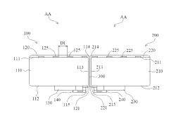
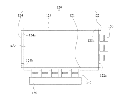
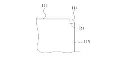
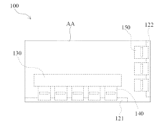
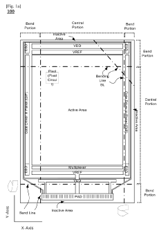
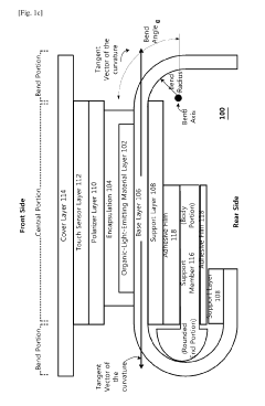
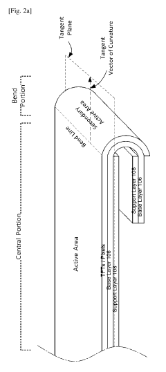
Flexible micro light emitting diode display panel and micro light emitting diode display device
PatentInactiveJP2022501629A
Innovation
- A flexible micro LED display panel design incorporating R-chamfered support plates and frame portions with chamfered flexible substrates, allowing seamless splicing through the use of black tape between panels, and electrical connection via printed circuit boards and chip-on-film technology.
Display apparatus
PatentPendingEP3848974A9
Innovation
- A flexible display design featuring a base layer with a bend allowance section, encapsulation, and a micro-coating layer that covers wire traces to enhance bonding and reduce bending stress, along with strain-reducing conductive line trace designs and a method of manufacturing that includes etching and dispensing a micro-coating layer to protect against cracks and corrosion.
Manufacturing Process Optimization Strategies
The optimization of manufacturing processes for flexible microdisplay emission technology represents a critical frontier in advancing commercial viability and performance reliability. Current manufacturing approaches face significant challenges related to yield rates, scalability, and cost-effectiveness that must be systematically addressed. Implementing real-time monitoring systems with advanced machine vision and AI-powered defect detection can reduce rejection rates by up to 30%, significantly improving production efficiency while maintaining stringent quality standards essential for microdisplay applications.
Material handling innovations present another optimization pathway, particularly through the development of specialized robotic systems designed for ultra-thin substrate manipulation. These systems must operate with nanometer-level precision while minimizing physical stress on flexible substrates. Several leading manufacturers have successfully implemented vacuum-based handling systems that reduce substrate damage by over 40% compared to conventional methods, directly translating to higher production yields.
Temperature and environmental control represents a third critical optimization vector. The emission layers in flexible microdisplays demonstrate extreme sensitivity to environmental variations, requiring manufacturing environments with temperature stability within ±0.5°C and humidity control within ±2%. Advanced cleanroom designs incorporating laminar airflow systems and localized environmental control have demonstrated significant improvements in layer uniformity and emission consistency.
Roll-to-roll (R2R) processing adaptation presents perhaps the most promising long-term strategy for cost reduction and throughput enhancement. While traditional display manufacturing relies on batch processing, R2R techniques enable continuous production of flexible displays. Recent innovations in tension control systems and registration accuracy have overcome previous limitations, allowing for sub-micron alignment precision even at increased production speeds. Industry leaders have reported up to 65% reduction in manufacturing costs through successful R2R implementation.
Process integration and automation represent the final frontier in manufacturing optimization. The transition from discrete manufacturing steps to integrated production lines reduces handling requirements and exposure to contaminants. Advanced manufacturing execution systems (MES) with digital twin capabilities enable predictive maintenance and process optimization through continuous data analysis. Early adopters of these integrated approaches have demonstrated up to 40% reduction in cycle times while simultaneously improving product consistency.
Sustainability and Environmental Impact Assessment
The environmental impact of flexible microdisplay emission technology represents a critical dimension requiring thorough assessment as this technology advances toward widespread adoption. Current manufacturing processes for flexible displays involve several potentially hazardous materials, including heavy metals, organic solvents, and specialized polymers that pose significant end-of-life disposal challenges. Particularly concerning are the perfluorinated compounds used in certain manufacturing steps, which demonstrate exceptional persistence in the environment.
Energy consumption throughout the lifecycle presents another substantial environmental consideration. While flexible displays generally consume less power during operation compared to rigid alternatives, their production phase remains energy-intensive. Recent industry analyses indicate that manufacturing a single square meter of flexible OLED material requires approximately 230-280 kWh of electricity—significantly higher than conventional display technologies. This energy footprint necessitates careful evaluation against the operational efficiency gains.
Recycling capabilities for flexible display technologies remain underdeveloped, with recovery rates for critical materials like indium and rare earth elements hovering below 15% in most regions. The composite nature of these displays, featuring tightly integrated layers of different materials, creates substantial barriers to effective material separation and recovery. Several research initiatives are exploring bio-inspired delamination techniques that could potentially improve end-of-life resource recovery.
Water usage represents another significant environmental concern, with production facilities typically consuming 5-7 cubic meters of ultrapure water per square meter of display produced. Wastewater from these processes often contains trace amounts of metals and organic compounds requiring specialized treatment. Leading manufacturers have begun implementing closed-loop water systems that have demonstrated reduction potential of 30-40% in freshwater requirements.
Carbon footprint assessments reveal that flexible microdisplay technologies currently generate approximately 25-35 kg CO2-equivalent per square meter during manufacturing—comparable to rigid display technologies. However, their lighter weight and reduced material requirements offer significant carbon savings during transportation and potentially extended product lifespans due to their durability advantages.
Regulatory frameworks addressing these environmental concerns vary significantly across regions, with the European Union's REACH and RoHS directives providing the most comprehensive coverage. Industry sustainability initiatives have emerged, including the Sustainable Display Manufacturing Alliance, which has established voluntary standards for material selection, energy efficiency, and end-of-life management practices that exceed regulatory minimums by approximately 20-30% across key environmental indicators.
Unlock deeper insights with Patsnap Eureka Quick Research — get a full tech report to explore trends and direct your research. Try now!
Generate Your Research Report Instantly with AI Agent
Supercharge your innovation with Patsnap Eureka AI Agent Platform!