Research on Semiconductor Layers in Flexible Microdisplays
OCT 21, 20259 MIN READ
Generate Your Research Report Instantly with AI Agent
Patsnap Eureka helps you evaluate technical feasibility & market potential.
Semiconductor Microdisplay Evolution and Objectives
The evolution of semiconductor technology in microdisplays has undergone significant transformation since the early 1990s, when the first microdisplay prototypes emerged. Initially, these displays utilized rigid silicon substrates with limited flexibility and relatively low resolution. The technological progression accelerated in the early 2000s with the introduction of low-temperature polysilicon (LTPS) technology, which enabled higher electron mobility and improved display performance while maintaining compatibility with flexible substrates.
By the mid-2010s, the industry witnessed a paradigm shift with the development of oxide semiconductor materials, particularly indium-gallium-zinc oxide (IGZO), which offered superior electron mobility compared to amorphous silicon while requiring lower processing temperatures. This breakthrough facilitated the integration of semiconductor layers onto flexible substrates without compromising performance, marking a critical milestone in flexible microdisplay development.
The current technological landscape is characterized by the exploration of organic semiconductors and two-dimensional materials such as graphene and transition metal dichalcogenides (TMDCs), which demonstrate exceptional mechanical flexibility and electrical properties. These materials are enabling unprecedented advancements in flexible microdisplay technology, with potential applications extending beyond traditional display markets.
The primary objective of semiconductor layer research in flexible microdisplays is to develop materials and fabrication processes that maintain high electron mobility and stability while accommodating mechanical deformation. This includes addressing challenges related to strain-induced performance degradation, interface quality between semiconductor and dielectric layers, and long-term reliability under repeated bending conditions.
Another critical goal is to reduce the processing temperature requirements for semiconductor deposition, enabling compatibility with a wider range of flexible substrate materials, including polymers with lower thermal stability thresholds. This would significantly expand the design possibilities and application scenarios for flexible microdisplays.
Furthermore, research aims to enhance the scalability of semiconductor layer fabrication processes, ensuring consistent performance across large-area displays while maintaining cost-effectiveness. This includes developing novel deposition techniques and patterning methods specifically optimized for flexible substrates.
The integration of additional functionalities within the semiconductor layer, such as sensing capabilities or energy harvesting, represents another important objective. This multifunctionality would enable the creation of more sophisticated flexible display systems that can interact with users and environments in novel ways, potentially revolutionizing human-machine interfaces and augmented reality experiences.
Market Analysis for Flexible Display Technologies
The flexible display market has experienced remarkable growth in recent years, with a global market value reaching $23.9 billion in 2022 and projected to surpass $86.7 billion by 2030, representing a compound annual growth rate (CAGR) of 17.4%. This exponential growth is primarily driven by increasing consumer demand for foldable smartphones, wearable devices, and other portable electronics that benefit from flexible display technologies.
Semiconductor layers play a crucial role in the performance and durability of flexible microdisplays. The market for specialized semiconductor materials used in these applications has seen significant expansion, with particular emphasis on organic semiconductors, metal oxide semiconductors, and low-temperature polysilicon (LTPS) technologies. These materials collectively represent a specialized market segment valued at approximately $3.2 billion in 2022.
Consumer electronics remains the dominant application sector, accounting for 68% of the flexible display market. However, automotive displays (12%), healthcare devices (8%), and military applications (7%) are rapidly growing segments that present substantial opportunities for semiconductor layer innovations. The remaining 5% encompasses emerging applications including smart home devices and retail displays.
Regionally, East Asia continues to dominate both production and consumption of flexible display technologies, with South Korea, Japan, and China collectively controlling 76% of global manufacturing capacity. North America and Europe represent significant consumer markets but have limited manufacturing presence, accounting for 14% and 8% of global production respectively.
Market analysis indicates that durability and performance remain the primary concerns for end-users of flexible display technologies. Specifically, semiconductor layers that can withstand repeated bending cycles while maintaining electrical performance command premium pricing, with manufacturers willing to pay 30-40% more for solutions that extend operational lifespan by at least 50%.
The competitive landscape is characterized by intense research and development activities, with major display manufacturers investing heavily in proprietary semiconductor layer technologies. Samsung Display, LG Display, and BOE Technology lead with the largest R&D budgets specifically allocated to flexible display semiconductor research, collectively spending over $4.3 billion annually on these initiatives.
Market forecasts suggest that innovations in semiconductor layers for flexible microdisplays will increasingly focus on transparency, energy efficiency, and compatibility with high-refresh-rate applications. Analysts predict that semiconductor solutions enabling fully transparent flexible displays will capture a premium market segment worth approximately $5.1 billion by 2025, representing one of the fastest-growing niches within the broader flexible display ecosystem.
Current Semiconductor Layer Fabrication Challenges
The fabrication of semiconductor layers for flexible microdisplays faces significant technical challenges that impede widespread commercial adoption. Traditional semiconductor manufacturing processes, optimized for rigid silicon substrates, are fundamentally incompatible with the temperature and mechanical constraints of flexible substrates. Polyimide and other flexible substrate materials typically cannot withstand temperatures above 350°C, whereas conventional semiconductor deposition often requires temperatures exceeding 600°C for optimal crystallization and electrical performance.
Low-temperature deposition techniques such as plasma-enhanced chemical vapor deposition (PECVD) and sputtering have been adapted for flexible displays, but these methods produce amorphous or polycrystalline semiconductor layers with inferior electron mobility compared to single-crystal materials. This mobility limitation directly impacts switching speed and power efficiency of the resulting display devices, creating a significant performance gap between flexible and conventional displays.
Uniformity across large areas presents another critical challenge. As display manufacturers push toward larger flexible panels, maintaining consistent semiconductor layer thickness and properties becomes increasingly difficult. Variations as small as a few nanometers can lead to visible brightness inconsistencies and pixel non-uniformity, severely affecting display quality. Current roll-to-roll processing techniques struggle to achieve the sub-nanometer precision required for high-resolution microdisplays.
Interface engineering between semiconductor layers and flexible substrates introduces additional complications. Thermal expansion coefficient mismatches create stress during temperature fluctuations, leading to delamination and cracking. Adhesion promoters and buffer layers can mitigate these issues but add process complexity and may introduce new electrical interface states that degrade device performance.
Encapsulation of semiconductor materials against oxygen and moisture represents a persistent challenge, as flexible barrier films typically have higher permeation rates than rigid glass encapsulation. Even trace amounts of environmental contaminants can rapidly degrade organic semiconductors and oxidize metal contacts, significantly reducing device lifetime. Current thin-film encapsulation technologies struggle to maintain the 10^-6 g/m²/day water vapor transmission rates required for OLED microdisplays while remaining flexible.
Scaling production from laboratory to industrial volumes introduces yield challenges unique to flexible semiconductor processing. Handling flexible substrates during multi-layer deposition requires specialized equipment to prevent wrinkling and contamination. Current manufacturing lines experience yield rates 15-20% lower than comparable rigid display production, substantially increasing costs and limiting market penetration of flexible microdisplay technologies.
Semiconductor Layer Deposition Techniques
01 Multilayer semiconductor structures
Multilayer semiconductor structures involve the deposition of multiple semiconductor layers with different compositions or properties to achieve specific electronic or optical characteristics. These structures can include various combinations of materials such as silicon, germanium, gallium arsenide, or compound semiconductors. The layering technique allows for the creation of quantum wells, superlattices, and heterojunctions that are essential for modern electronic and optoelectronic devices.- Multilayer semiconductor structures: Multilayer semiconductor structures involve the deposition of different semiconductor materials in layers to create specific electronic properties. These structures are fundamental in creating various semiconductor devices such as transistors, diodes, and integrated circuits. The layering technique allows for precise control of electrical characteristics by manipulating the composition, thickness, and doping of each layer, enabling the development of high-performance electronic components.
- Magnetic and memory semiconductor applications: Semiconductor layers are crucial in magnetic storage and memory applications. These specialized layers can be engineered to exhibit magnetic properties or to function as part of memory storage devices. The integration of semiconductor materials with magnetic components enables the development of high-density storage solutions, magnetic sensors, and non-volatile memory technologies that combine the benefits of semiconductor processing with magnetic data retention capabilities.
- Protective and functional coating layers: Semiconductor devices often incorporate protective and functional coating layers that shield the active components from environmental factors while enhancing performance. These layers can include passivation films, insulating barriers, and specialized coatings that prevent oxidation, moisture ingress, or mechanical damage. Additionally, functional coatings can provide specific optical, thermal, or electrical properties that improve device efficiency and reliability under various operating conditions.
- Thermal management in semiconductor layers: Effective thermal management is essential in semiconductor layer design to prevent performance degradation and failure due to heat buildup. Specialized semiconductor layers can be engineered to dissipate heat efficiently or to provide thermal isolation between components. These thermal management solutions may include the integration of high thermal conductivity materials, the creation of heat-spreading layers, or the implementation of thermal barrier coatings to maintain optimal operating temperatures in semiconductor devices.
- Advanced deposition techniques for semiconductor layers: The quality and performance of semiconductor devices heavily depend on the techniques used to deposit the semiconductor layers. Advanced deposition methods such as atomic layer deposition, molecular beam epitaxy, and chemical vapor deposition enable precise control over layer thickness, composition, and crystallinity. These techniques allow for the creation of ultra-thin films, complex heterostructures, and defect-free interfaces that are essential for next-generation semiconductor devices with enhanced functionality and efficiency.
02 Semiconductor layer deposition techniques
Various techniques are employed for depositing semiconductor layers, including chemical vapor deposition (CVD), molecular beam epitaxy (MBE), atomic layer deposition (ALD), and sputtering. These methods allow precise control over layer thickness, composition, and crystallinity. The choice of deposition technique significantly impacts the quality and properties of the semiconductor layers, affecting the performance of the resulting devices.Expand Specific Solutions03 Magnetic and memory applications of semiconductor layers
Semiconductor layers are crucial in magnetic storage and memory applications. These include magnetic tunnel junctions, spin valves, and other spintronic devices where semiconductor layers are combined with magnetic materials. The interaction between semiconductor and magnetic layers enables the development of high-density storage media, magnetic random access memory (MRAM), and other advanced memory technologies with improved performance characteristics.Expand Specific Solutions04 Semiconductor layers in optoelectronic devices
Semiconductor layers are fundamental components in optoelectronic devices such as light-emitting diodes (LEDs), photodetectors, and solar cells. By engineering the bandgap and other properties of semiconductor layers, devices can be designed to emit or absorb light at specific wavelengths. Multiple semiconductor layers with varying compositions create quantum wells that enhance light emission efficiency or absorption characteristics, leading to improved device performance.Expand Specific Solutions05 Doping and modification of semiconductor layers
Doping and modification techniques are used to alter the electrical, optical, and structural properties of semiconductor layers. These include ion implantation, thermal diffusion, and in-situ doping during growth. Additionally, post-deposition treatments such as annealing, etching, and surface passivation can be applied to optimize layer properties. These modifications enable the creation of p-n junctions, ohmic contacts, and other essential components of semiconductor devices.Expand Specific Solutions
Leading Manufacturers and Research Institutions
The flexible microdisplay semiconductor layer market is in a growth phase, characterized by increasing demand for wearable devices, AR/VR applications, and foldable displays. The market is projected to reach significant scale as technology matures from current experimental to commercial applications. Leading players include Samsung Display, LG Display, and BOE Technology Group, who have established strong positions through extensive R&D investments and patent portfolios. Japanese firms like Sharp and JDI contribute significant technological expertise, while emerging Chinese manufacturers such as Tianma Microelectronics and TCL CSOT are rapidly advancing their capabilities. Academic-industry partnerships with institutions like MIT and KAIST are accelerating innovation in novel materials and fabrication techniques for next-generation flexible displays.
BOE Technology Group Co., Ltd.
Technical Solution: BOE has developed advanced semiconductor layer technologies specifically for flexible microdisplays, focusing on low-temperature polysilicon (LTPS) and oxide thin-film transistor (TFT) backplanes. Their proprietary Flexible OLED (FOLED) technology utilizes ultra-thin semiconductor layers with thickness below 50nm to achieve flexibility while maintaining electrical performance. BOE has pioneered a unique semiconductor transfer process that allows for the deposition of high-quality silicon-based semiconductors onto flexible polymer substrates at temperatures below 200°C, preserving substrate integrity while achieving electron mobility exceeding 30 cm²/Vs[1]. Their flexible displays incorporate specialized buffer layers between the semiconductor and substrate to minimize stress during bending, enabling radius curvatures of less than 1mm without performance degradation[2]. BOE has also developed specialized encapsulation technologies using alternating inorganic/organic thin films to protect the sensitive semiconductor layers from oxygen and moisture penetration, extending flexible display lifetime significantly.
Strengths: Industry-leading production capacity for flexible displays with established mass manufacturing processes; proprietary semiconductor deposition techniques allowing for higher temperature processing on flexible substrates. Weaknesses: Higher production costs compared to rigid display technologies; challenges in achieving uniform semiconductor layer performance across large flexible surfaces.
SAMSUNG DISPLAY CO LTD
Technical Solution: Samsung Display has pioneered advanced semiconductor layer technologies for flexible microdisplays through their Y-OCTA (Youm On-Cell Touch AMOLED) technology. This approach integrates touch sensors directly into the display panel's thin-film encapsulation (TFE) layer, eliminating the need for additional touch films and reducing overall thickness to under 60μm[3]. Their flexible displays utilize low-temperature polycrystalline oxide (LTPO) semiconductor backplanes that combine oxide TFT and LTPS technologies, enabling variable refresh rates from 1-120Hz while minimizing power consumption. Samsung has developed proprietary Ultra-Thin Glass (UTG) technology with specialized semiconductor buffer layers that distribute stress evenly during flexing operations, allowing for over 200,000 fold cycles without significant performance degradation[4]. Their semiconductor layers incorporate nano-scale stress-relief structures that prevent crack propagation during bending. Additionally, Samsung has implemented multi-layer thin-film encapsulation with alternating inorganic/organic films (typically SiNx and polyacrylates) with total thickness below 3μm to protect semiconductor layers while maintaining flexibility.
Strengths: Industry-leading Ultra-Thin Glass (UTG) technology providing superior protection for semiconductor layers while maintaining flexibility; advanced LTPO backplane technology enabling variable refresh rates and power efficiency. Weaknesses: Higher production complexity and costs; challenges in scaling manufacturing to larger display sizes while maintaining semiconductor layer uniformity.
Key Patents in Flexible Semiconductor Materials
Flexible display using semiconductor light-emitting device and method of manufacturing the same
PatentInactiveUS20070152577A1
Innovation
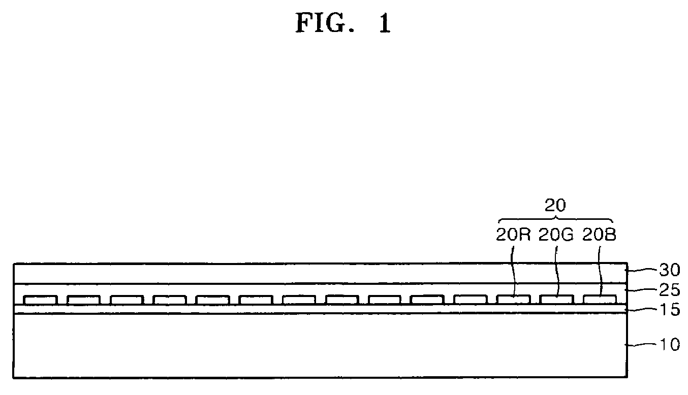
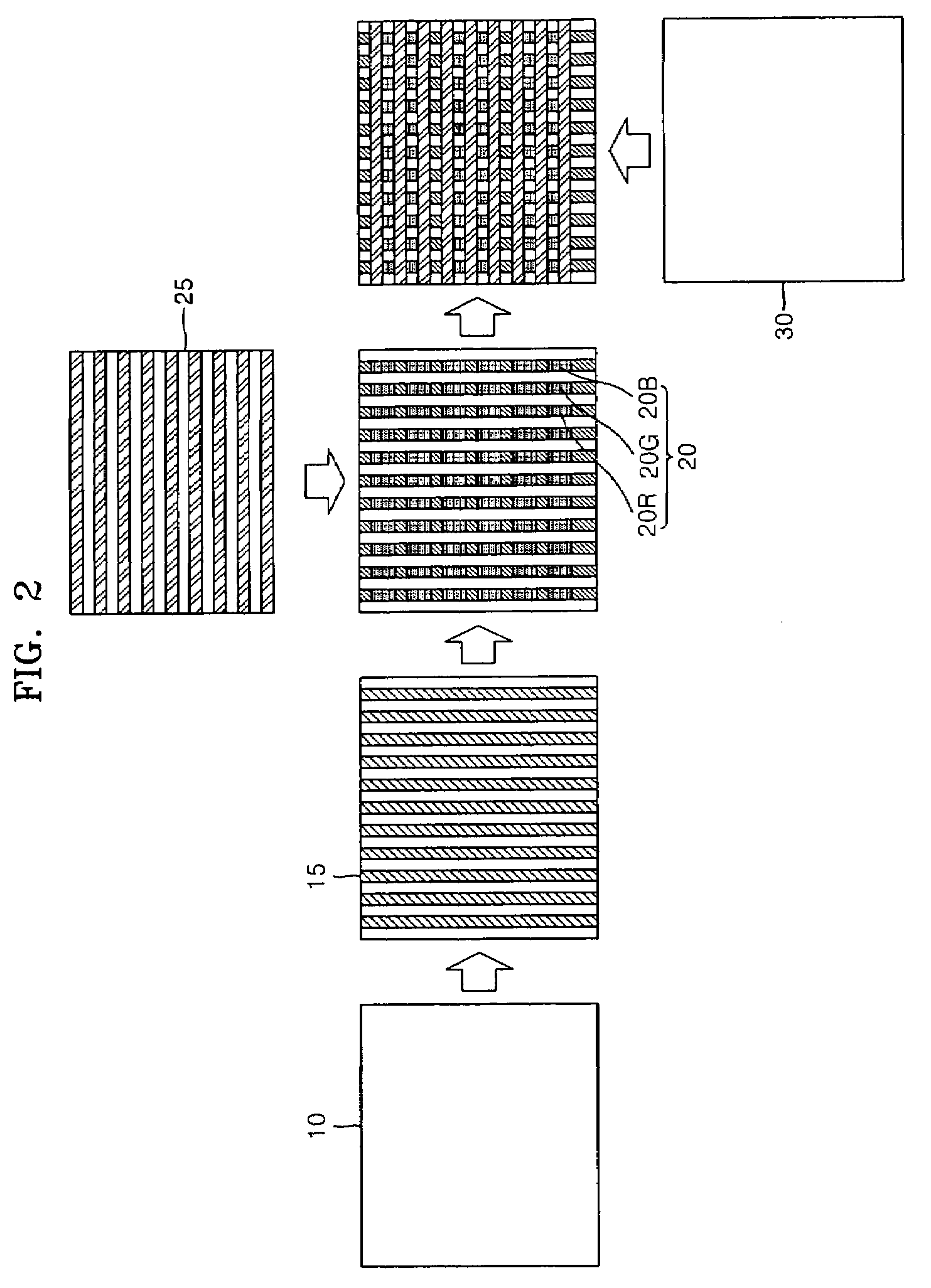
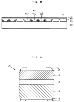
- A flexible display using a semiconductor light-emitting device with a flexible plastic substrate, metal or conductive polymeric circuit layers, and a light-transmissive capping layer, where semiconductor light-emitting devices are arranged in pixels with a specific area ratio to ensure high emission efficiency and long lifespan.
Flexible display device
PatentActiveUS11908871B2
Innovation
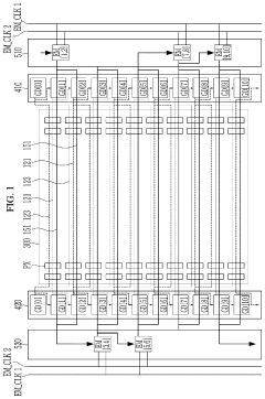
- Incorporating a transistor with an asymmetric channel structure, where the channel width varies along the channel region, and a gate electrode that overlaps the channel region, to distribute electrical stress and maintain output current under mechanical stress.
Supply Chain Considerations for Flexible Displays
The flexible display supply chain presents unique challenges and opportunities compared to traditional rigid display manufacturing. Material sourcing for semiconductor layers in flexible microdisplays requires specialized suppliers capable of producing ultra-thin, bendable semiconductor materials with consistent quality. Currently, the supply chain is concentrated in East Asia, with South Korea, Japan, and Taiwan dominating the production of key components such as flexible substrates, thin-film transistors, and organic light-emitting materials.
Manufacturing processes for flexible displays demand specialized equipment that differs significantly from conventional display production lines. This equipment scarcity creates potential bottlenecks in scaling production, with only a limited number of manufacturers capable of producing the precision tools required for flexible semiconductor layer deposition. The geographical concentration of these equipment suppliers primarily in Japan and Germany introduces geopolitical vulnerabilities to the supply chain.
Yield management represents a critical challenge in flexible display production. The handling of ultra-thin semiconductor materials during manufacturing processes results in significantly lower yields compared to rigid displays, often 15-20% lower in initial production runs. This yield gap directly impacts cost structures and production planning, requiring manufacturers to implement specialized quality control measures throughout the supply chain.
Transportation and logistics for flexible display components require careful consideration due to the delicate nature of the materials. Specialized packaging solutions and controlled environment shipping are necessary to prevent damage to semiconductor layers during transit. These requirements add complexity and cost to the supply chain, particularly for global distribution networks spanning multiple climate zones.
Inventory management strategies must be adapted for flexible display components due to their shorter shelf life compared to traditional semiconductor materials. The reactive nature of some organic semiconductor compounds necessitates just-in-time manufacturing approaches, reducing buffer inventory possibilities and increasing supply chain vulnerability to disruptions.
Vertical integration has emerged as a strategic approach among leading manufacturers to mitigate supply chain risks. Companies like Samsung Display and LG Display have invested in controlling multiple stages of the production process, from material synthesis to final assembly. This approach provides greater control over quality and supply security but requires substantial capital investment that smaller players cannot match, potentially leading to further industry consolidation.
Reliability Testing Methodologies
Reliability testing methodologies for semiconductor layers in flexible microdisplays require comprehensive approaches that address the unique challenges posed by bendable substrates and dynamic operating conditions. These methodologies can be categorized into mechanical stress testing, environmental durability assessment, and electrical performance verification under various conditions.
Mechanical reliability testing includes cyclic bending tests where samples undergo repeated flexing at controlled radii (typically 1-10mm) for thousands to millions of cycles. Tensile and compressive stress measurements quantify the semiconductor layer's ability to maintain structural integrity during deformation. Three-point and four-point bending tests provide standardized measurements of flexibility thresholds before electrical or physical failure occurs.
Environmental reliability assessment involves temperature cycling tests (-40°C to 85°C) to evaluate thermal expansion mismatch effects between semiconductor layers and flexible substrates. Humidity resistance testing (85°C/85% RH) examines moisture penetration impacts on semiconductor performance. Additionally, accelerated aging tests simulate long-term operational conditions to predict lifetime performance degradation of the semiconductor materials.
Electrical reliability verification encompasses bias-temperature stress testing, where semiconductor layers are subjected to electrical bias under elevated temperatures to assess performance stability. Constant current stress tests evaluate electromigration resistance in flexible configurations. Importantly, these electrical tests must be performed while the display is in both flat and bent states to comprehensively characterize performance.
Advanced reliability methodologies incorporate in-situ monitoring techniques that allow real-time observation of failure mechanisms during testing. Acoustic emission detection identifies microscopic fractures in semiconductor layers during bending. Electrical impedance spectroscopy tracks changes in semiconductor properties throughout reliability testing cycles. These approaches provide deeper insights into failure modes and degradation mechanisms.
Standardization efforts by organizations such as JEDEC, IEC, and SEMI are establishing uniform testing protocols specifically for flexible electronics. These include modified versions of traditional semiconductor reliability tests adapted for flexible substrates, with particular attention to the semiconductor-substrate interface behavior under mechanical stress.
Correlation studies between accelerated testing and real-world usage patterns are essential for translating laboratory results into meaningful lifetime predictions. Mathematical models incorporating Weibull distribution analysis and Monte Carlo simulations help predict failure rates and establish reliability benchmarks for semiconductor layers in commercial flexible display applications.
Unlock deeper insights with Patsnap Eureka Quick Research — get a full tech report to explore trends and direct your research. Try now!
Generate Your Research Report Instantly with AI Agent
Supercharge your innovation with Patsnap Eureka AI Agent Platform!

