

Analysis of OLED vs MicroLED in Consumer Electronics
OCT 24, 20259 MIN READ
Generate Your Research Report Instantly with AI Agent
Patsnap Eureka helps you evaluate technical feasibility & market potential.
OLED and MicroLED Technology Evolution and Objectives
Display technology has undergone significant evolution since the introduction of cathode ray tubes (CRTs) in the early 20th century. The transition from CRTs to liquid crystal displays (LCDs) marked the first major shift toward flatter, more energy-efficient screens. OLED (Organic Light-Emitting Diode) technology emerged in the late 1980s, with the first practical OLED device developed by Eastman Kodak in 1987. This innovation represented a fundamental departure from LCD technology by eliminating the need for backlighting, as each pixel in an OLED display emits its own light.
The commercial adoption of OLED displays began in the early 2000s, initially in small devices like MP3 players and mobile phones. By the 2010s, OLED technology had matured sufficiently to be incorporated into larger displays, including televisions and computer monitors. The technology's ability to deliver perfect blacks, wide viewing angles, and vibrant colors positioned it as a premium display solution for high-end consumer electronics.
MicroLED technology represents the next evolutionary step in display technology. Unlike OLEDs, which use organic compounds that degrade over time, MicroLEDs utilize inorganic gallium nitride (GaN) materials, offering potentially longer lifespans and higher brightness levels. The concept of MicroLED was first demonstrated in the early 2000s, but manufacturing challenges prevented commercial viability until recently.
The technical objectives for both OLED and MicroLED technologies align with broader industry goals: achieving higher resolution, improved energy efficiency, extended lifespan, and enhanced color accuracy. However, each technology pursues these objectives through different approaches. OLED development focuses on addressing inherent limitations such as burn-in susceptibility and limited brightness, while MicroLED research concentrates on overcoming manufacturing complexities and cost barriers.
Current technological trajectories suggest a future where OLED and MicroLED coexist in different market segments. OLED technology continues to dominate in mobile devices and premium televisions, while MicroLED is positioned to excel in applications requiring extreme brightness, durability, and scalability, such as large-format displays and outdoor signage.
The ultimate objective for both technologies is to achieve the perfect display: one that combines infinite contrast, perfect color reproduction, maximum energy efficiency, unlimited lifespan, and manufacturing scalability at competitive price points. As research continues, we can expect incremental improvements in existing OLED technology while MicroLED gradually overcomes its production challenges to become more commercially viable across a wider range of consumer electronics.
Consumer Electronics Display Market Analysis
The consumer electronics display market has witnessed significant transformation over the past decade, primarily driven by technological advancements in display technologies. Currently, the market is dominated by LCD (Liquid Crystal Display) and OLED (Organic Light Emitting Diode) technologies, with MicroLED emerging as a promising contender. The global display market was valued at approximately $148 billion in 2022 and is projected to reach $206 billion by 2027, growing at a CAGR of 6.8%.
OLED displays have gained substantial market share in premium smartphones and high-end televisions, with Samsung and LG leading production. In 2022, OLED displays accounted for roughly 30% of the smartphone display market and 15% of the premium television market. The technology's ability to deliver perfect blacks, vibrant colors, and flexible form factors has made it particularly attractive for flagship devices.
MicroLED, though still in early commercialization stages, is generating significant interest from major electronics manufacturers. The technology promises superior brightness (up to 5,000 nits compared to OLED's typical 1,000 nits), longer lifespan (approximately 100,000 hours versus OLED's 30,000-60,000 hours), and improved energy efficiency. Market penetration remains minimal, with less than 1% market share, primarily in ultra-premium televisions and specialized applications.
Consumer preferences are increasingly favoring thinner devices with edge-to-edge displays, higher resolution, and better color accuracy. This trend has accelerated the adoption of OLED in smartphones, with approximately 70% of premium smartphones now featuring OLED displays. Additionally, foldable displays, enabled by OLED technology, have created a new product category that is expected to grow at 35% annually through 2026.
Regional analysis reveals Asia-Pacific as the dominant manufacturing hub, with South Korea, Japan, and China accounting for over 75% of global display production. North America and Europe represent the largest consumer markets for premium display technologies, while emerging economies show rapid growth in adoption of mid-range display solutions.
The supply chain for advanced display technologies remains complex and vulnerable to disruptions. The recent semiconductor shortage highlighted dependencies on specialized components, with production delays affecting multiple consumer electronics segments. For MicroLED specifically, manufacturing challenges related to mass transfer techniques and yield rates continue to impact production costs and scalability.
Looking forward, the display market is expected to see increased competition between OLED and MicroLED technologies in premium segments, while LCD will likely maintain dominance in mid-range and budget devices. Technological convergence may also emerge, with hybrid solutions incorporating elements from multiple display technologies to optimize performance and cost.
Current Technical Limitations and Challenges
Despite significant advancements in both OLED and MicroLED technologies, several technical limitations and challenges persist that impact their widespread adoption in consumer electronics. OLED technology, while mature in many aspects, continues to face issues with burn-in, where static images displayed for extended periods cause permanent damage to organic compounds. This particularly affects devices displaying static elements like status bars or channel logos. Additionally, OLED panels demonstrate limited brightness capabilities compared to competing technologies, with peak brightness typically capped around 1,000-1,500 nits, restricting their performance in bright ambient conditions.
Manufacturing scalability remains a significant challenge for OLED, particularly for larger displays. The yield rates for large OLED panels are relatively low, contributing to higher production costs that are ultimately passed on to consumers. Furthermore, the organic materials in OLED displays are susceptible to degradation over time, resulting in color shifts and reduced luminance, which impacts the long-term consistency of display quality.
MicroLED technology faces even more substantial manufacturing hurdles. The process of precisely placing millions of microscopic LEDs onto a substrate with near-perfect accuracy presents unprecedented engineering challenges. Current manufacturing processes struggle with mass transfer techniques that can efficiently and reliably position these tiny components without defects. The yield rates for MicroLED displays remain extremely low, especially as pixel densities increase for higher resolution displays.
Cost factors represent a major barrier to MicroLED adoption in mainstream consumer electronics. The complex manufacturing processes and specialized equipment required result in production costs that are prohibitively high for most consumer applications. Industry estimates suggest MicroLED displays currently cost 5-10 times more than equivalent OLED panels, limiting their market presence primarily to premium or specialized products.
Power efficiency presents different challenges for each technology. While OLED offers excellent power efficiency for dark content due to its ability to completely turn off individual pixels, it becomes less efficient when displaying bright content. Conversely, MicroLED promises better overall efficiency but currently struggles with power management at the individual pixel level, particularly in smaller form factors like smartphones and wearables.
Heat dissipation represents another significant technical challenge, especially for MicroLED. The high current densities required to drive these displays can generate substantial heat, necessitating advanced thermal management solutions that add complexity and cost to device designs. This becomes particularly problematic in compact devices where space for cooling systems is limited.
For both technologies, achieving consistent color reproduction across the entire display area remains challenging. Manufacturing variations can lead to noticeable differences in brightness and color accuracy between different regions of the same display, requiring sophisticated compensation algorithms and quality control processes.
Comparative Analysis of OLED vs MicroLED Solutions
01 OLED Display Technology Advancements
Organic Light Emitting Diode (OLED) technology has evolved significantly with improvements in efficiency, brightness, and lifespan. These displays utilize organic compounds that emit light when an electric current is applied. Recent advancements include flexible OLED panels, transparent displays, and enhanced color gamut capabilities. The technology offers advantages such as perfect black levels, high contrast ratios, and reduced power consumption compared to traditional LCD displays.- OLED display structure and materials: OLED (Organic Light Emitting Diode) displays utilize organic compounds that emit light when electricity is applied. These displays feature multiple layers including cathode, emissive layer, conductive layer, and anode. The technology offers advantages such as self-illumination, flexibility, and high contrast ratios. Various organic materials are used to produce different colors, and the structure can be optimized for improved efficiency and lifespan.
- MicroLED fabrication and integration: MicroLED technology involves the fabrication and integration of microscopic LED arrays to create displays. The manufacturing process includes epitaxial growth, transfer printing, and bonding techniques to place tiny LED chips onto display substrates. These displays offer high brightness, energy efficiency, and long lifespans. The integration challenges include precise alignment of microLEDs and establishing reliable electrical connections across the display panel.
- Display driving and control systems: Advanced driving and control systems are essential for both OLED and MicroLED displays. These systems include thin-film transistor (TFT) backplanes, driver ICs, and control algorithms that manage pixel addressing, brightness control, and power management. The driving schemes can be active or passive matrix, with active matrix providing better performance for high-resolution displays. Specialized circuits are implemented to compensate for variations in pixel performance and to extend display lifetime.
- Pixel architecture and color management: The pixel architecture in OLED and MicroLED displays determines resolution, color accuracy, and power efficiency. Different subpixel arrangements (RGB, RGBW, PenTile) are used to optimize specific display characteristics. Color management systems include calibration techniques, color filters, and quantum dot enhancement layers to achieve wide color gamuts. Advanced pixel designs incorporate features for high dynamic range (HDR) content and reduced power consumption during partial display usage.
- Flexible and transparent display technologies: Both OLED and MicroLED technologies can be adapted for flexible and transparent display applications. These displays use specialized substrates such as polyimide films or ultra-thin glass that can bend without breaking. Transparent displays incorporate see-through electrodes and light-emitting materials. Manufacturing processes include low-temperature deposition techniques and encapsulation methods to protect sensitive components from oxygen and moisture while maintaining flexibility or transparency.
02 MicroLED Display Innovations
MicroLED displays represent the next generation of display technology, utilizing microscopic LED arrays that are self-emissive. These displays offer superior brightness, energy efficiency, and longer lifespans compared to other technologies. Recent innovations focus on manufacturing processes to reduce production costs, improve yield rates, and enable mass production of these displays for consumer electronics applications. MicroLED technology provides exceptional picture quality with high dynamic range and wide color gamut.Expand Specific Solutions03 Display Integration and Form Factors
Both OLED and MicroLED technologies are enabling new form factors and integration possibilities in electronic devices. Innovations include foldable displays, rollable screens, and curved panels that can be incorporated into various consumer electronics. These flexible form factors are made possible by the thin, lightweight nature of these display technologies. Additionally, advancements in bezel-less designs and under-display components are creating more immersive viewing experiences.Expand Specific Solutions04 Manufacturing Processes and Materials
Significant advancements have been made in the manufacturing processes and materials used for both OLED and MicroLED displays. These include improved deposition techniques, novel substrate materials, and enhanced encapsulation methods to protect sensitive components. Innovations in transfer processes for MicroLED pixels and improved organic materials for OLED displays have addressed previous limitations in mass production. These manufacturing improvements are critical for reducing costs and increasing adoption of these advanced display technologies.Expand Specific Solutions05 Power Efficiency and Control Systems
Both OLED and MicroLED display technologies feature advanced power management and control systems to optimize energy consumption while maintaining display quality. Innovations include pixel-level power control, adaptive brightness technologies, and sophisticated driving circuits. These systems enable more efficient operation, extending battery life in portable devices while reducing heat generation. Additionally, advancements in backplane technologies and thin-film transistors have improved the overall performance and reliability of these display technologies.Expand Specific Solutions
Key Industry Players and Ecosystem
The OLED vs MicroLED competition in consumer electronics is currently in a transitional phase, with OLED technology dominating the market while MicroLED emerges as a promising challenger. The global display market is valued at approximately $150 billion, with OLED capturing a significant share due to its maturity and widespread adoption. Samsung, LG Display, and BOE Technology lead OLED production with established manufacturing capabilities and product integration. MicroLED technology, though less mature, is gaining momentum with companies like Samsung, Apple, and Lumileds investing heavily in R&D. The technology gap is narrowing as manufacturers like TCL China Star Optoelectronics and Intel develop innovative solutions to address MicroLED's manufacturing challenges, particularly in miniaturization and mass production efficiency.
BOE Technology Group Co., Ltd.
Technical Solution: BOE has emerged as China's leading display manufacturer with significant investments in both OLED and MicroLED technologies. For OLED, BOE operates multiple flexible AMOLED production lines with monthly capacity exceeding 144,000 substrates. Their OLED technology incorporates advanced pixel compensation circuits to address uniformity issues and extend panel lifespan. BOE has developed a proprietary "MLED" (Mini/Micro LED) technology platform that utilizes a mass transfer process capable of handling millions of microscopic LED chips simultaneously. Their MicroLED approach features pixel pitches ranging from 0.4mm to 1.5mm for different applications, with brightness capabilities exceeding 1,500 nits while maintaining power efficiency. BOE has also pioneered hybrid solutions that combine quantum dot color conversion layers with MicroLED backplanes to improve color performance while reducing manufacturing complexity.
Strengths: Rapidly expanding production capacity; strong government support; competitive pricing strategy. Weaknesses: Still catching up to Korean manufacturers in yield rates for premium OLED panels; MicroLED mass production techniques still being refined.
Samsung Electronics Co., Ltd.
Technical Solution: Samsung has pioneered both OLED and MicroLED technologies for consumer electronics. For OLED, Samsung utilizes its proprietary AMOLED technology in smartphones and tablets, with recent advancements in QD-OLED (Quantum Dot OLED) for premium TVs that combine quantum dots with OLED to enhance color volume and brightness while maintaining perfect blacks. In MicroLED, Samsung has commercialized "The Wall" - modular MicroLED displays using inorganic LED chips smaller than 100 micrometers that self-emit light without requiring backlighting. Samsung's MicroLED implementation features millions of individual RGB microscopic LED chips that emit their own light, achieving brightness levels up to 2,000 nits while maintaining 100% color volume of DCI-P3 color gamut. Their latest iterations have reduced the pixel pitch to under 0.6mm for consumer applications.
Strengths: Vertical integration from component manufacturing to end products; proprietary mass production techniques for both technologies; strong IP portfolio. Weaknesses: High manufacturing costs for MicroLED limiting mainstream adoption; OLED still faces burn-in issues and shorter lifespan compared to traditional LCD technologies.
Critical Patents and Technical Innovations
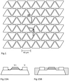
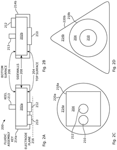
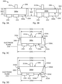
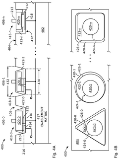
Encapsulated light emitting diodes for selective fluidic assembly
PatentActiveUS12119432B2
Innovation
- The use of partially encapsulated semiconductor-based inorganic micro-LEDs with a patternable polymer encapsulant that protects the LEDs from collisions and optimizes their shape for efficient assembly, allowing for higher speed and yield while preventing defects, and enabling precise alignment of LED colors on a display substrate.
Anisotropic conductive film and display device
PatentActiveUS20220102326A1
Innovation
- An anisotropic conductive film with a first region of discretely arranged conductive particles corresponding to electrode patterns and a second region with aggregated conductive particles acting as an alignment marker, facilitating easy alignment with the circuit substrate and reducing production costs by forming alignment markers through conductive particle dispersion.
Manufacturing Process and Scalability Assessment
The manufacturing processes for OLED and MicroLED technologies represent critical factors in their commercial viability and market adoption. OLED manufacturing has matured significantly over the past decade, with established production methods including vacuum thermal evaporation for small molecule OLEDs and solution processing for polymer-based variants. Major manufacturers like Samsung and LG Display have achieved economies of scale through substantial investments in production facilities, resulting in gradually decreasing production costs, though still higher than conventional LCD manufacturing.
OLED production faces persistent challenges including material degradation during manufacturing, yield issues particularly for larger panels, and the need for precise deposition control. These factors contribute to higher production costs that are reflected in consumer pricing. The industry has developed specialized techniques such as fine metal masks for RGB patterning and thin film encapsulation to address these challenges, but manufacturing complexity remains a barrier to further cost reduction.
MicroLED manufacturing, by contrast, remains in early development stages with significant scalability challenges. The process involves the precise placement of millions of microscopic LED chips, each measuring less than 100 micrometers, requiring unprecedented precision in mass production environments. Current manufacturing approaches include monolithic integration, mass transfer techniques, and pick-and-place methods, each with distinct advantages and limitations for different applications and display sizes.
The most significant manufacturing hurdle for MicroLED is the mass transfer process - moving millions of tiny LED chips from growth substrates to display backplanes with near-perfect yield. Companies like Apple, Samsung, and specialized firms such as PlayNitride and Jade Bird Display are developing proprietary solutions, including stamp transfer methods, laser transfer techniques, and fluid-assisted assembly. However, these processes have not yet demonstrated commercial viability at consumer electronics scales.
Yield management represents another critical challenge, as defect rates must approach zero for viable consumer products. Even minimal defect rates can result in visible display imperfections, necessitating either perfect initial placement or effective repair mechanisms. Current repair processes are time-consuming and expensive, limiting production throughput and scalability.
Equipment infrastructure for MicroLED manufacturing is still evolving, with specialized tools being developed by companies like Applied Materials and Veeco. The capital expenditure required for establishing MicroLED production lines exceeds that of OLED facilities, creating a significant barrier to entry for new market participants and slowing industry-wide adoption.
While OLED manufacturing has achieved commercial scale with ongoing optimization, MicroLED production remains at the prototype and small-batch stage, with at least 3-5 years required before reaching the maturity needed for mainstream consumer electronics adoption at competitive price points.
Energy Efficiency and Environmental Impact
Energy efficiency represents a critical factor in the comparison between OLED and MicroLED technologies for consumer electronics. OLED displays demonstrate variable power consumption patterns directly correlated with content being displayed. Dark or black content requires minimal power as individual pixels can be completely turned off, while bright scenes demand significantly more energy. This self-emissive characteristic gives OLED an advantage in applications where dark content predominates.
MicroLED technology, while still evolving, shows promising energy efficiency characteristics. Current implementations indicate that MicroLED displays can achieve up to 30% greater energy efficiency than comparable OLED panels when displaying mixed content. This efficiency stems from superior light emission properties and reduced heat generation during operation, potentially extending battery life in portable devices.
The manufacturing processes for both technologies present distinct environmental considerations. OLED production involves organic compounds and solvents that require careful handling and disposal. The industry has made significant strides in reducing harmful chemicals, with major manufacturers implementing closed-loop recycling systems that recover up to 95% of certain solvents used in production.
MicroLED manufacturing currently demands more energy-intensive processes, particularly in the precise placement of millions of microscopic LEDs. However, the longer theoretical lifespan of MicroLED displays (potentially exceeding 100,000 hours versus 30,000-50,000 for OLED) may offset initial production impacts through reduced replacement frequency and electronic waste generation.
End-of-life considerations reveal further distinctions. OLED panels contain organic materials that degrade naturally but may include potentially harmful heavy metals in certain components. MicroLED displays contain fewer toxic substances overall but present recycling challenges due to the miniaturized components and complex assembly methods.
Carbon footprint analyses across the full lifecycle indicate that current OLED technology generates approximately 12-15% less carbon emissions during manufacturing compared to early MicroLED production. However, when accounting for energy consumption during use and extended lifespan, MicroLED displays may achieve a lower lifetime carbon footprint in applications with high daily usage patterns exceeding five hours.
Water usage represents another environmental factor, with OLED manufacturing typically consuming 30-40% less water than current MicroLED production processes, though this gap is narrowing as manufacturing techniques evolve and scale.
Unlock deeper insights with Patsnap Eureka Quick Research — get a full tech report to explore trends and direct your research. Try now!
Generate Your Research Report Instantly with AI Agent
Supercharge your innovation with Patsnap Eureka AI Agent Platform!