

Benchmarking FinFET Robustness In Variable Environments
SEP 11, 20259 MIN READ
Generate Your Research Report Instantly with AI Agent
PatSnap Eureka helps you evaluate technical feasibility & market potential.
FinFET Technology Evolution and Objectives
FinFET technology emerged as a revolutionary advancement in semiconductor manufacturing, addressing the limitations of planar transistors as device dimensions continued to shrink below 22nm. Since its commercial introduction by Intel in 2011, FinFET has evolved through multiple generations, each bringing significant improvements in performance, power efficiency, and density. The three-dimensional fin structure allows for better electrostatic control of the channel, substantially reducing leakage current and short-channel effects that plagued traditional MOSFET designs.
The evolution of FinFET technology can be traced through several key milestones. The first-generation 22nm FinFETs demonstrated the viability of the architecture for high-volume manufacturing. Subsequent generations at 14nm, 10nm, and 7nm nodes have progressively refined the fin geometry, gate stack materials, and manufacturing processes to enhance performance metrics. Recent advancements have focused on improving fin aspect ratios, reducing parasitic capacitance, and implementing strain engineering techniques to boost carrier mobility.
Current objectives in FinFET development center around enhancing robustness in variable operating environments. As these devices are deployed in increasingly diverse applications—from data centers to automotive systems to IoT devices—they must maintain reliable performance across wide temperature ranges, voltage fluctuations, and radiation exposure conditions. Benchmarking FinFET robustness has therefore become critical for predicting device behavior in real-world scenarios.
The primary technical goals include developing standardized methodologies for assessing FinFET reliability under environmental stress, quantifying performance degradation mechanisms, and establishing design guidelines for environment-specific optimizations. Particular emphasis is placed on understanding how variable environments affect critical parameters such as threshold voltage stability, subthreshold swing, and hot carrier degradation.
Looking forward, the industry aims to extend FinFET technology to its physical limits while simultaneously exploring transition paths to alternative architectures like Gate-All-Around (GAA) FETs. The benchmarking of environmental robustness will play a crucial role in determining the viability of FinFETs for next-generation applications with stringent reliability requirements, such as autonomous vehicles, medical implants, and aerospace systems.
The ultimate objective is to establish comprehensive models that can accurately predict FinFET behavior across the entire operating envelope, enabling designers to implement appropriate compensation mechanisms and reliability-enhancing features at the circuit and system levels.
Market Demand Analysis for Robust FinFET Solutions
The semiconductor industry's demand for robust FinFET solutions has been growing exponentially as electronic devices continue to penetrate diverse environments. Market research indicates that the global FinFET technology market is projected to reach $35 billion by 2026, with a compound annual growth rate of approximately 22% from 2021. This substantial growth is primarily driven by the increasing need for high-performance computing solutions across variable operating conditions.
The automotive sector represents one of the most significant market segments demanding robust FinFET solutions. With the rise of autonomous vehicles and advanced driver assistance systems, semiconductors must maintain reliability across extreme temperature ranges (-40°C to 150°C) and withstand vibration, humidity, and electromagnetic interference. The automotive semiconductor market specifically for robust FinFET solutions is expected to grow at 25% annually through 2025.
Consumer electronics manufacturers are increasingly seeking FinFET technologies that can maintain performance consistency across diverse usage scenarios. As smartphones, tablets, and wearables are used in environments ranging from arctic expeditions to desert conditions, the ability to benchmark and guarantee performance across these variables has become a critical purchasing factor for semiconductor buyers.
Data center operators represent another major market segment driving demand for environmentally robust FinFET solutions. With the trend toward edge computing and distributed data centers, chips are increasingly deployed in less controlled environments compared to traditional data centers. This shift has created a premium market for FinFETs that can maintain performance and power efficiency across varying humidity, temperature, and power quality conditions.
The aerospace and defense sectors have particularly stringent requirements for semiconductor performance in extreme environments. These industries demand FinFET solutions that can withstand radiation exposure, extreme temperature cycling, and high-altitude conditions. Though smaller in volume compared to consumer markets, this segment commands premium pricing for qualified solutions, with contracts often valued 3-5 times higher than commercial equivalents.
Industrial IoT applications are emerging as a significant growth driver for robust FinFET solutions. As connected sensors and processing units are deployed in manufacturing facilities, agricultural settings, and infrastructure monitoring, the ability to maintain consistent performance across dust, chemical exposure, and temperature variations has become essential. Market analysis shows this segment growing at 30% annually, representing one of the fastest-expanding applications for environmentally robust FinFETs.
Current FinFET Robustness Challenges in Variable Environments
FinFET technology has revolutionized semiconductor manufacturing, but its robustness faces significant challenges in variable environments. Temperature fluctuations represent one of the most critical issues, as FinFET performance characteristics exhibit strong temperature dependence. At elevated temperatures, carrier mobility decreases while leakage current increases, leading to performance degradation and potential reliability issues. Conversely, at extremely low temperatures, threshold voltage shifts and carrier freeze-out phenomena can occur, affecting circuit functionality.
Voltage variations present another major challenge. As supply voltages continue to scale down to reduce power consumption, FinFETs become increasingly sensitive to voltage fluctuations. Even minor voltage droops can cause timing violations in high-performance circuits, while voltage overshoots may accelerate device aging mechanisms such as Bias Temperature Instability (BTI) and Hot Carrier Injection (HCI).
Process variations inherent in manufacturing introduce additional robustness concerns. Fin width and height variations significantly impact threshold voltage uniformity across a chip. With fin dimensions approaching sub-10nm, atomic-level variations become increasingly problematic, leading to device-to-device performance mismatches that complicate circuit design and reduce yield.
Radiation effects pose a growing challenge for FinFETs in aerospace, military, and even some commercial applications. Single Event Upsets (SEUs) can flip stored bits in memory cells, while Total Ionizing Dose (TID) effects gradually degrade device performance over time. The three-dimensional structure of FinFETs, while beneficial for electrostatic control, creates complex radiation interaction paths that are difficult to model and mitigate.
Aging mechanisms represent a long-term robustness concern. BTI causes threshold voltage shifts over time, particularly under elevated temperature and voltage conditions. HCI damages the gate oxide near the drain, gradually degrading device performance. Time-Dependent Dielectric Breakdown (TDDB) eventually leads to gate oxide failure. These reliability issues are exacerbated in variable environments where temperature and voltage fluctuations accelerate aging processes.
Electrostatic discharge (ESD) vulnerability remains a significant challenge. The thin gate oxide and reduced thermal mass of FinFET structures make them particularly susceptible to ESD damage. Traditional protection schemes must be carefully redesigned to accommodate the unique characteristics of FinFET devices without compromising performance or area efficiency.
Mechanical stress effects, both intentional (for performance enhancement) and unintentional (from packaging), impact FinFET robustness. While controlled stress can improve carrier mobility, uncontrolled stress variations can lead to unpredictable performance shifts and reliability concerns, particularly in applications subject to mechanical vibration or thermal cycling.
Current Benchmarking Methodologies for FinFET Robustness
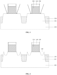
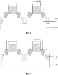
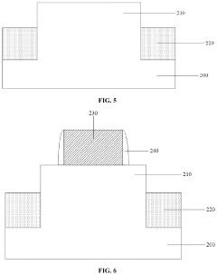
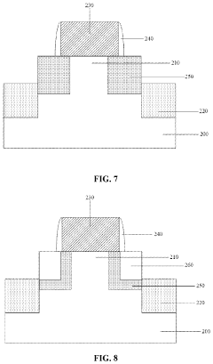
01 Structural design enhancements for FinFET robustness
Various structural modifications can be implemented to enhance FinFET robustness, including optimized fin geometry, improved gate stack configurations, and novel channel materials. These design enhancements help to reduce short channel effects, minimize leakage current, and improve overall device performance under varying operational conditions. Structural robustness improvements also address issues related to mechanical stress and thermal stability, which are critical for long-term reliability.- Structural design enhancements for FinFET robustness: Various structural modifications can be implemented to enhance FinFET robustness. These include optimizing fin dimensions, implementing stress-relief features, and improving gate structure designs. Such structural enhancements help to reduce mechanical stress, prevent fin collapse, and improve overall device reliability under various operating conditions. These design considerations are critical for maintaining performance stability and extending device lifetime in advanced semiconductor applications.
- Process optimization techniques for robust FinFET fabrication: Specialized fabrication processes can significantly improve FinFET robustness. These include optimized etching techniques, precise doping profiles, and advanced deposition methods that enhance uniformity and reduce defects. Process optimization focuses on creating consistent fin structures with minimal variation, improving gate oxide quality, and ensuring proper metal contact formation. These techniques collectively contribute to manufacturing robust FinFETs with improved yield and reliability.
- Circuit design techniques for FinFET robustness: Circuit-level approaches can enhance FinFET robustness through specialized design methodologies. These include redundancy schemes, adaptive biasing techniques, and noise-tolerant circuit configurations. By implementing robust circuit designs that account for FinFET-specific characteristics, designers can mitigate the effects of process variations, temperature fluctuations, and aging effects. These techniques help maintain circuit performance and reliability throughout the device lifetime.
- Thermal management solutions for FinFET reliability: Thermal management is crucial for maintaining FinFET robustness under various operating conditions. Techniques include implementing heat dissipation structures, thermal-aware layout designs, and dynamic thermal management systems. These solutions help prevent performance degradation due to self-heating effects, which are particularly pronounced in FinFET structures due to their 3D geometry. Effective thermal management extends device lifetime and ensures consistent performance across a wide range of applications.
- Radiation and environmental hardening for FinFETs: Specialized techniques can enhance FinFET robustness against radiation and harsh environmental conditions. These include implementing guard rings, using radiation-hardened materials, and employing specialized layout techniques that minimize charge collection from radiation events. Such approaches are particularly important for FinFETs used in aerospace, military, and other high-reliability applications where exposure to radiation and extreme environmental conditions is expected.
02 Process optimization techniques for robust FinFET manufacturing
Advanced manufacturing processes can significantly improve FinFET robustness through precise control of critical dimensions, improved doping profiles, and enhanced etching techniques. These optimizations help to reduce process variations that can lead to device performance inconsistencies. Key process improvements include refined lithography techniques, controlled fin formation processes, and optimized annealing steps that collectively enhance device yield and reliability across different operational environments.Expand Specific Solutions03 Circuit design techniques for FinFET robustness
Circuit-level design approaches can enhance FinFET robustness by implementing redundancy, error correction mechanisms, and adaptive biasing schemes. These techniques help mitigate the impact of process variations and environmental factors on circuit performance. Advanced layout strategies, including careful consideration of device orientation and placement, can also improve resistance to various failure mechanisms while maintaining optimal performance characteristics under different operating conditions.Expand Specific Solutions04 Reliability enhancement methods for FinFET devices
Specific reliability enhancement methods focus on addressing common FinFET failure mechanisms such as hot carrier injection, bias temperature instability, and time-dependent dielectric breakdown. These methods include specialized stress testing protocols, aging models, and reliability-aware design approaches. Implementation of protective structures and guard rings can also improve electrostatic discharge protection and reduce susceptibility to latch-up, thereby enhancing overall device robustness under extreme conditions.Expand Specific Solutions05 Novel materials and interfaces for robust FinFET performance
Introduction of novel materials and interface engineering techniques can significantly improve FinFET robustness. High-k dielectric materials, metal gates with optimized work functions, and strain-engineered channels contribute to enhanced device performance and reliability. Advanced contact materials and improved isolation techniques also play crucial roles in reducing parasitic effects and improving thermal management, which are essential aspects of maintaining robust performance across varying operational conditions and extended device lifetimes.Expand Specific Solutions
Leading Semiconductor Companies in FinFET Technology
The FinFET robustness benchmarking landscape is currently in a mature growth phase, with the market expanding as semiconductor manufacturers seek solutions for variable environment challenges. The global market is estimated at $5-7 billion, driven by increasing demand for reliable high-performance chips in automotive and IoT applications. Leading players include TSMC, Samsung, and Intel, who have established advanced FinFET technologies at 7nm and below. SMIC and GlobalFoundries are making significant progress in developing competitive solutions, while research institutions like Xidian University and IMEC are contributing breakthrough innovations. Qualcomm, NXP, and Texas Instruments are focusing on application-specific optimizations to enhance FinFET performance across temperature and voltage variations.
Taiwan Semiconductor Manufacturing Co., Ltd.
Technical Solution: TSMC has developed comprehensive FinFET benchmarking methodologies to evaluate robustness across variable environments. Their approach includes multi-variable stress testing that examines FinFET performance under extreme temperature ranges (-40°C to 125°C), voltage variations (±10% nominal), and different process corners. TSMC's 5nm and 3nm FinFET technologies incorporate self-heating effect (SHE) models that account for thermal variations in high-density circuits. Their reliability testing framework includes electromigration (EM) and time-dependent dielectric breakdown (TDDB) assessments under variable environmental conditions. TSMC has implemented statistical element variation modeling that captures both systematic and random variations in FinFET structures, allowing for accurate Monte Carlo simulations to predict yield and performance across environmental variables.
Strengths: Industry-leading process technology with extensive real-world manufacturing data for validation; comprehensive modeling capabilities that account for multiple environmental variables simultaneously. Weaknesses: Proprietary benchmarking methodologies limit academic collaboration; higher implementation costs compared to less advanced nodes.
International Business Machines Corp.
Technical Solution: IBM has pioneered advanced FinFET benchmarking methodologies focusing on environmental variability through their Predictive Technology Model (PTM) framework. Their approach integrates machine learning algorithms with traditional SPICE simulations to predict FinFET performance across temperature (-55°C to 125°C), humidity (10-95% RH), and radiation exposure conditions. IBM's benchmarking includes specialized radiation hardening assessments for aerospace and military applications, measuring Single Event Upsets (SEUs) and Total Ionizing Dose (TID) effects on FinFET structures. Their Environmental Stress Screening (ESS) methodology applies accelerated life testing principles to identify early failure mechanisms in variable environments. IBM has also developed unique benchmarking for cryogenic computing environments (below 4K), supporting quantum computing integration with FinFET control electronics.
Strengths: Exceptional research depth with strong academic partnerships; specialized expertise in extreme environment applications including aerospace and quantum computing. Weaknesses: Less focus on high-volume consumer applications; benchmarking methodologies sometimes prioritize scientific exploration over manufacturing efficiency.
Key Patents and Research on Environmental Variability Compensation
Stress in n-channel field effect transistors
PatentWO2016018514A2
Innovation
- A method involving a gate stack on a semiconductor fin with a conductive gate and dielectric layer, where a stressor material is deposited and confined by a capping material to apply compressive or tensile stress along the fin's height, enhancing carrier mobility by altering the stressor material's volume through processes like disruptive structural phase transition, silicidation, or oxidation.
Fin field-effect transistor having counter-doped regions between lightly doped regions and doped source/drain regions
PatentActiveUS11114551B2
Innovation
- A method involving lightly doped regions and counter doped regions formed through specific ion implantation processes to reduce the ion concentration gradient between doped source/drain regions and lightly doped regions, thereby mitigating the GIDL phenomenon.
Thermal Management Strategies for FinFET Devices
Thermal management has emerged as a critical challenge in FinFET technology due to the increasing power densities and thermal issues that arise from device scaling. As FinFET dimensions continue to shrink, the heat generated per unit area increases significantly, leading to potential reliability concerns and performance degradation. Effective thermal management strategies are therefore essential to ensure optimal device performance across variable environmental conditions.
Several approaches have been developed to address thermal challenges in FinFET devices. Advanced packaging solutions incorporating thermal interface materials (TIMs) with enhanced thermal conductivity have shown promising results in facilitating heat dissipation from the active device regions. These materials, including metal-based TIMs and carbon nanotube composites, provide efficient thermal pathways that significantly reduce junction temperatures under high-load conditions.
Dynamic thermal management (DTM) techniques represent another crucial strategy, employing real-time monitoring and adaptive control mechanisms to regulate device temperatures. These systems utilize embedded thermal sensors to detect temperature fluctuations and trigger appropriate responses such as frequency scaling, voltage adjustments, or workload migration to cooler regions of the chip. Recent benchmarking studies have demonstrated that DTM implementations can reduce peak temperatures by up to 15°C while maintaining performance within 5% of optimal levels.
Microfluidic cooling technologies have also gained traction for high-performance FinFET applications. These systems integrate microscale fluid channels directly into the chip packaging or substrate, enabling localized cooling at hotspots. Experimental results indicate that microfluidic cooling can achieve thermal resistances below 0.1 K/W, substantially outperforming conventional air cooling solutions in variable environmental conditions.
Novel substrate materials with enhanced thermal properties represent a fundamental approach to thermal management. Silicon-on-diamond (SOD) and silicon-on-aluminum nitride (SoAlN) substrates have demonstrated thermal conductivities 3-5 times higher than conventional silicon substrates, effectively mitigating self-heating effects in FinFET devices. Benchmarking studies across temperature ranges from -40°C to 125°C show that these advanced substrates maintain more consistent device characteristics throughout operational environmental variations.
3D integration techniques with through-silicon vias (TSVs) offer additional thermal management benefits by providing direct thermal pathways from heat-generating components to heat sinks. However, careful design considerations are necessary as TSVs can introduce thermal stress that impacts FinFET reliability. Recent robustness tests indicate that optimized TSV placement can reduce thermal gradients by up to 40% while minimizing stress-induced performance variations.
Process Variation Impact on FinFET Performance
Process variations represent one of the most significant challenges in FinFET manufacturing and performance optimization. As transistor dimensions continue to shrink below 10nm, even minor deviations in the fabrication process can substantially impact device characteristics and circuit performance. These variations manifest in multiple dimensions, including fin width fluctuations, gate length variability, and oxide thickness inconsistencies, all of which directly affect threshold voltage, leakage current, and switching speed.
Statistical analysis of modern FinFET processes reveals that process-induced variations can cause up to 30% deviation in drive current and threshold voltage across a single wafer. This variability becomes particularly problematic in high-performance computing applications where timing margins are increasingly constrained. Temperature-dependent effects further compound these variations, with performance metrics showing different sensitivity to process variations across operating temperature ranges.
The impact of process variations on FinFET performance exhibits distinct patterns across different technology nodes. At 16nm and 14nm nodes, gate length variations predominantly affect performance, while at 10nm and 7nm nodes, fin width variations become increasingly dominant. This shift necessitates evolving strategies for variation-aware design methodologies as technology scales further.
Systematic variations, resulting from lithography limitations, etching non-uniformities, and chemical-mechanical polishing inconsistencies, contribute approximately 60% of the total variation budget in current FinFET technologies. The remaining 40% stems from random variations, including random dopant fluctuations and line edge roughness, which become increasingly significant at advanced nodes due to the reduced number of dopant atoms in the channel region.
Multi-gate architectures in FinFETs provide inherent advantages in variation tolerance compared to planar technologies, with improved electrostatic control reducing the impact of channel length variations. However, this benefit is partially offset by the introduction of new variation sources unique to 3D structures, such as fin height variability and sidewall angle inconsistencies.
Advanced process control techniques have demonstrated capability to reduce systematic variations by up to 40% in production environments. These include feed-forward control systems, real-time monitoring, and adaptive lithography techniques. Despite these improvements, the fundamental physics of atomic-scale manufacturing ensures that variation management, rather than elimination, remains the practical approach for robust FinFET implementation.
Unlock deeper insights with PatSnap Eureka Quick Research — get a full tech report to explore trends and direct your research. Try now!
Generate Your Research Report Instantly with AI Agent
Supercharge your innovation with PatSnap Eureka AI Agent Platform!