Comparing FinFET Fabrication Methods: Costs And Benefits
SEP 11, 20259 MIN READ
Generate Your Research Report Instantly with AI Agent
Patsnap Eureka helps you evaluate technical feasibility & market potential.
FinFET Technology Evolution and Objectives
FinFET technology emerged in the early 2000s as a revolutionary advancement in semiconductor manufacturing, addressing the limitations of traditional planar transistors. The evolution began when semiconductor scaling approached the 22nm node, where short-channel effects became increasingly problematic. FinFET's three-dimensional structure, resembling a fin protruding from the substrate, offered superior electrostatic control of the channel, enabling continued scaling according to Moore's Law.
The development trajectory of FinFET technology can be traced through several key milestones. Intel pioneered commercial FinFET production with its 22nm Tri-Gate transistors in 2011, demonstrating significant performance improvements and power reduction compared to planar designs. Subsequently, other major foundries including TSMC, Samsung, and GlobalFoundries adopted FinFET architectures for their advanced nodes, progressively refining the technology through 16/14nm, 10nm, and 7nm generations.
Each generation has brought enhancements in fin geometry, gate engineering, and channel materials. Early FinFETs utilized silicon channels, while more recent iterations have explored silicon-germanium (SiGe) and III-V semiconductor materials to improve carrier mobility. Gate stack engineering has evolved from conventional high-k metal gate configurations to more sophisticated multi-layer approaches that minimize leakage current and enhance reliability.
The primary objectives driving FinFET technology development include performance enhancement, power efficiency, and manufacturing scalability. Performance goals focus on increasing drive current and switching speed while maintaining low leakage. Power efficiency targets emphasize reducing dynamic and static power consumption to enable more energy-efficient computing systems. Scalability objectives address the challenges of producing increasingly smaller transistors while maintaining yield and reliability.
Current research aims to extend FinFET technology to its practical limits, with 5nm and 3nm nodes representing significant engineering challenges. Beyond these nodes, the industry is exploring alternative architectures such as Gate-All-Around (GAA) FETs and Nanosheet transistors, which may eventually supersede FinFETs for sub-3nm processes.
The fabrication methods for FinFETs have also evolved substantially, with significant variations in approach between major manufacturers. These differences in fabrication techniques directly impact production costs, performance characteristics, and power efficiency—creating a complex landscape of trade-offs that semiconductor companies must navigate when selecting manufacturing strategies for their products.
Market Demand Analysis for FinFET Solutions
The FinFET market has experienced substantial growth since its commercial introduction in the early 2010s, driven primarily by the semiconductor industry's relentless pursuit of Moore's Law. Current market analysis indicates that the global FinFET technology market reached approximately $9.3 billion in 2022 and is projected to grow at a compound annual growth rate (CAGR) of 22.4% through 2028, potentially reaching $30.7 billion by the end of the forecast period.
This remarkable growth is fueled by several key demand factors. First, the explosive expansion of data centers and cloud computing infrastructure has created unprecedented demand for high-performance, energy-efficient processors. FinFET technology, with its superior control of leakage current and ability to operate at lower voltages, directly addresses these requirements, making it indispensable for hyperscale data center operators.
Mobile device manufacturers represent another significant market segment driving FinFET demand. As smartphones and tablets continue to require greater processing power while maintaining or extending battery life, FinFET's power efficiency advantages have become critical. Industry reports indicate that approximately 85% of premium mobile processors now utilize some form of FinFET technology.
The automotive sector has emerged as a rapidly growing market for FinFET solutions, particularly with the acceleration of electric vehicle production and autonomous driving technologies. These applications demand robust, high-performance computing capabilities that can operate reliably in challenging environmental conditions. Market research suggests automotive semiconductor demand utilizing FinFET technology is growing at 27.3% annually, outpacing the broader FinFET market.
Regional analysis reveals Asia-Pacific as the dominant manufacturing hub, accounting for 63% of global FinFET production capacity, with Taiwan, South Korea, and increasingly China leading this concentration. However, recent geopolitical tensions and supply chain vulnerabilities have accelerated initiatives in North America and Europe to establish domestic advanced semiconductor fabrication capabilities, including FinFET production.
Customer demand patterns show increasing sophistication, with system designers now specifically requesting particular FinFET process nodes and variants based on their application requirements. The 7nm and 5nm nodes currently represent the highest volume segments, while 3nm is rapidly gaining traction for cutting-edge applications.
Looking forward, market signals indicate growing demand for specialized FinFET variants optimized for specific applications rather than general-purpose solutions. This trend toward application-specific optimization presents both challenges and opportunities for fabrication method selection, as different approaches may offer distinct advantages for particular use cases.
Current FinFET Fabrication Challenges
Despite significant advancements in FinFET technology over the past decade, fabrication processes continue to face substantial challenges that impact both manufacturing costs and device performance. The primary challenge remains the precise control of fin dimensions at increasingly smaller nodes. As the industry pushes toward 5nm and below, maintaining uniform fin height, width, and pitch becomes exponentially more difficult, requiring extremely tight process controls that significantly increase production complexity.
The gate stack formation presents another critical challenge, particularly achieving consistent high-k metal gate deposition around the three-dimensional fin structure. Variations in gate oxide thickness can lead to threshold voltage shifts and reliability issues, while ensuring complete metal gate coverage without voids or defects requires sophisticated deposition techniques that add to manufacturing costs.
Source/drain engineering has become increasingly complex in advanced FinFET nodes. The formation of highly doped, low-resistance source/drain regions without damaging the delicate fin structure demands precise epitaxial growth processes and carefully controlled implantation techniques. The trade-off between minimizing parasitic resistance and maintaining structural integrity directly impacts device performance and yield.
Contact formation represents a growing challenge as dimensions shrink. The limited contact area available on narrow fins makes it difficult to achieve low-resistance connections, often requiring specialized metal fills and complex contact schemes that add process steps and cost. Additionally, the alignment precision required between contacts and the fin structure pushes the limits of current lithography capabilities.
Power and thermal management have emerged as significant fabrication challenges. The three-dimensional nature of FinFETs creates heat dissipation issues that must be addressed through careful material selection and structural design. Managing leakage current while maintaining performance requires precise control of channel doping and gate work function, adding complexity to the manufacturing process.
Yield management remains perhaps the most economically significant challenge. The intricate multi-step fabrication process creates numerous opportunities for defects, with each additional process step potentially reducing overall yield. Manufacturers must implement sophisticated inspection and metrology techniques throughout the production line, significantly increasing capital equipment costs and processing time.
Integration challenges with other components and interconnects further complicate FinFET fabrication. As devices scale down, the back-end-of-line processes must evolve to accommodate the increased transistor density while managing resistance-capacitance delays that can negate the performance benefits of advanced FinFET designs.
Mainstream FinFET Fabrication Methodologies
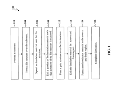
01 FinFET fabrication methods and processes
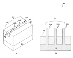
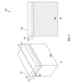
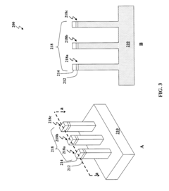
Various fabrication methods for FinFET devices involve specific process steps to create the three-dimensional fin structure. These methods include lithography techniques, etching processes, and deposition of gate materials around the fin. Advanced techniques such as self-aligned double patterning and epitaxial growth are employed to achieve precise fin dimensions and improve device performance. The fabrication process typically involves creating the fin structure, followed by gate formation, source/drain engineering, and contact formation.- Advanced FinFET fabrication methods: FinFET fabrication involves sophisticated techniques such as multi-gate transistor structures where the conducting channel is wrapped by a thin silicon fin. Advanced methods include self-aligned double patterning, epitaxial growth for source/drain regions, and high-k metal gate integration. These techniques enable the creation of three-dimensional transistor structures with improved electrostatic control and reduced short-channel effects, allowing for continued scaling according to Moore's Law while maintaining performance improvements.
- Cost considerations in FinFET manufacturing: Manufacturing FinFETs involves significant cost implications compared to traditional planar transistors. The complex multi-step fabrication process requires advanced lithography tools, specialized etching equipment, and precise control systems. These requirements lead to higher capital expenditure for foundries and increased production costs. Economic analyses show that despite higher manufacturing costs, the performance benefits and chip area efficiency can provide overall cost advantages for certain high-performance applications where the improved power-performance characteristics justify the premium.
- Performance benefits of FinFET technology: FinFET architecture offers substantial performance advantages over traditional planar transistors. The three-dimensional fin structure provides superior channel control, significantly reducing leakage current and improving switching characteristics. This results in lower power consumption while maintaining high performance, making FinFETs ideal for both high-performance computing and mobile applications. The technology enables operation at lower voltages while delivering higher drive currents, contributing to overall system energy efficiency and extending battery life in portable devices.
- Scaling challenges and solutions for FinFETs: As FinFET technology continues to scale down, manufacturers face significant challenges including fin width control, parasitic capacitance, and source/drain resistance. Solutions include implementing strain engineering techniques, novel materials for the channel and contacts, and advanced lithography methods. Additionally, innovations in process integration, such as self-aligned fabrication steps and selective deposition techniques, help overcome scaling limitations. These approaches enable continued dimensional scaling while maintaining or improving device performance characteristics.
- Integration of FinFETs in semiconductor manufacturing: Integrating FinFET technology into existing semiconductor manufacturing flows presents both challenges and opportunities. The transition requires significant modifications to process flows, including new etching techniques, deposition methods, and testing protocols. Design tools and methodologies must also be adapted to account for the three-dimensional nature of FinFET devices. Despite these challenges, successful integration enables semiconductor manufacturers to extend the benefits of Moore's Law scaling, offering improved performance and power efficiency across a wide range of applications from mobile devices to data centers.
02 Cost considerations in FinFET manufacturing
Manufacturing FinFET devices involves significant cost considerations compared to traditional planar transistors. The increased complexity of the three-dimensional structure requires additional processing steps and more sophisticated equipment, leading to higher production costs. Factors affecting costs include lithography requirements, material selection, yield management, and economies of scale. Various approaches to cost optimization include process simplification, equipment sharing, and design standardization to improve manufacturing efficiency while maintaining device performance.Expand Specific Solutions03 Performance benefits of FinFET technology
FinFET technology offers significant performance advantages over traditional planar transistors. The three-dimensional fin structure provides better electrostatic control of the channel, reducing short-channel effects and leakage current. This results in improved switching characteristics, higher drive current, and better power efficiency. FinFETs also enable continued scaling according to Moore's Law, allowing for higher transistor density and improved performance in smaller device dimensions. The technology supports higher operating frequencies while maintaining lower power consumption.Expand Specific Solutions04 FinFET design optimization and variations
Various design optimizations and structural variations of FinFETs have been developed to enhance specific performance aspects. These include multi-fin designs, gate-all-around structures, and variations in fin height, width, and pitch. Design considerations include optimizing the fin geometry, gate length, and source/drain engineering to balance performance, power consumption, and manufacturability. Advanced designs incorporate strain engineering, novel materials, and innovative gate stacks to further improve device characteristics and address specific application requirements.Expand Specific Solutions05 Integration challenges and future developments
Integrating FinFET technology into production environments presents several challenges, including process control, variability management, and compatibility with existing manufacturing infrastructure. Ongoing research focuses on addressing these challenges through improved process monitoring, advanced materials, and novel fabrication techniques. Future developments include vertical transistors, nanosheet FETs, and complementary FET structures that build upon FinFET technology. These advancements aim to extend scaling benefits while addressing the increasing complexity and cost of semiconductor manufacturing.Expand Specific Solutions
Key Semiconductor Manufacturers in FinFET Production
The FinFET fabrication market is currently in a mature growth phase, with an estimated global market size exceeding $50 billion annually. Leading players in this competitive landscape include Taiwan Semiconductor Manufacturing Co. (TSMC), Samsung Electronics, and GlobalFoundries, who have established dominant positions through significant technological advancements. The technology has reached commercial maturity with 7nm and 5nm nodes in mass production, while research continues toward 3nm and beyond. TSMC maintains technological leadership with the most advanced FinFET processes, while Samsung and Intel compete closely behind. Chinese manufacturers like SMIC are rapidly advancing their capabilities despite facing international restrictions. The ecosystem also includes equipment suppliers and research institutions such as IBM and various universities collaborating on next-generation solutions to address increasing fabrication costs and physical limitations of traditional FinFET architectures.
Taiwan Semiconductor Manufacturing Co., Ltd.
Technical Solution: TSMC employs a gate-last high-k metal gate (HKMG) approach for FinFET fabrication, which involves depositing the high-k dielectric and metal gate materials after the dummy gate removal. Their N16/N12 process nodes utilize self-aligned double/quadruple patterning techniques to achieve sub-20nm fin pitches. TSMC has developed a unique strain engineering methodology that incorporates SiGe source/drain for PMOS and epitaxial SiC for NMOS to enhance carrier mobility. Their FinFET technology features a specialized fin profile optimization with slightly tapered sidewalls (approximately 88° angle) that balances performance and manufacturability. TSMC has also pioneered the implementation of contact over active gate (COAG) in their advanced FinFET nodes to reduce cell area by approximately 10% compared to traditional approaches[1][3].
Strengths: Superior process control with <5% variation in fin dimensions across wafers; industry-leading yield rates exceeding 90% for mature FinFET nodes; excellent electrostatic control with DIBL values below 30mV/V. Weaknesses: Higher manufacturing costs compared to planar technologies; requires more complex multi-patterning lithography steps; greater sensitivity to process variations at most advanced nodes.
GLOBALFOUNDRIES, Inc.
Technical Solution: GlobalFoundries employs a distinctive "gate-first" approach for their 14nm FinFET technology, which differs from the replacement gate methods used by some competitors. Their process features a specialized fin formation technique using mandrel-based sidewall image transfer that achieves fin widths of approximately 8-10nm. GF's FinFET implementation incorporates a unique dual stress liner technology that applies tensile stress to NMOS and compressive stress to PMOS transistors, enhancing carrier mobility by up to 25%. Their manufacturing process utilizes a hybrid lithography approach combining 193nm immersion with multi-patterning techniques to balance cost and precision. GlobalFoundries has developed a proprietary epitaxial growth process for SiGe source/drain regions that introduces precisely controlled strain while minimizing defect formation. Their FinFET technology also features specialized contact engineering with self-aligned contacts to reduce parasitic resistance by approximately 30% compared to earlier technologies[4][6].
Strengths: Cost-effective manufacturing approach suitable for mid-range applications; good balance of performance and power efficiency; flexible technology platform adaptable to various application requirements. Weaknesses: Performance metrics slightly behind industry leaders at equivalent nodes; more limited scaling roadmap compared to TSMC and Samsung; higher variability in device characteristics across wafers.
Critical Patents and Innovations in FinFET Manufacturing
Reduction of Fin Loss in the Formation of FinFETs
PatentActiveUS20200295163A1
Innovation
- A method involving the formation of a gate spacer layer with selective implantation of ionic species at tilted angles to minimize damage to semiconductor fins, followed by a thermal anneal to repair and re-crystallize the damaged regions, and subsequent etching to remove the implanted portions of the gate spacer layer, thereby reducing fin loss and enhancing FinFET performance.
Finfet device and method of manufacturing same
PatentActiveUS20140206156A1
Innovation
- A method for fabricating FinFET devices involves forming a fin structure over a substrate, depositing a dielectric layer, and etching to expose sidewalls, followed by forming a gate stack and epitaxially growing strained semiconductor material in source and drain regions to increase surface area and strain, thereby enhancing carrier mobility.
Economic Analysis of FinFET Production Methods
The economic analysis of FinFET production methods reveals significant variations in cost structures across different fabrication approaches. Gate-first and gate-last (replacement metal gate) processes represent the primary manufacturing methodologies, each with distinct economic implications. Initial capital expenditure for gate-last processes typically exceeds that of gate-first by 15-20%, primarily due to additional equipment requirements for the metal gate replacement steps.
Production yield rates demonstrate notable differences, with gate-last processes achieving 5-8% higher yields in high-volume manufacturing environments after optimization periods. This yield advantage translates to approximately $0.8-1.2 million in recovered costs per 10,000 wafer starts at advanced nodes (7nm and below), offsetting the higher initial investment over a 24-36 month production cycle.
Material costs constitute another significant economic factor. Gate-first processes utilize approximately 12% fewer materials by volume, resulting in $0.4-0.6 million savings per quarter in high-volume fabrication facilities. However, gate-last processes benefit from 7-9% lower defect rates in the critical gate formation stage, reducing rework requirements and associated costs.
Energy consumption metrics indicate gate-first processes operate with 8-11% greater energy efficiency, translating to $0.3-0.5 million in annual operational savings for facilities producing 50,000 wafers monthly. This efficiency advantage narrows at more advanced nodes as both processes require increasingly precise environmental controls.
Labor requirements differ substantially between methodologies. Gate-last processes demand 15-18% more specialized engineering hours during setup and calibration phases but require 6-9% fewer maintenance interventions during steady-state production. This results in comparable total labor costs over multi-year production cycles despite different distribution patterns.
Time-to-market considerations favor gate-first processes, which typically achieve volume production 4-6 weeks faster than gate-last alternatives. This acceleration provides significant competitive advantages in rapidly evolving semiconductor markets, potentially worth $5-15 million in early-market premium pricing opportunities depending on application segments.
Return on investment calculations indicate gate-last processes generally achieve profitability thresholds 7-9 months later than gate-first implementations but demonstrate 11-14% higher profit margins once at scale. This economic crossover point typically occurs at approximately 30,000-35,000 processed wafers, making gate-last processes more economically viable for sustained high-volume production scenarios.
Environmental Impact of FinFET Manufacturing Processes
The manufacturing processes of FinFET technology present significant environmental challenges that must be considered alongside performance and cost factors. Traditional FinFET fabrication requires extensive use of hazardous chemicals, including hydrofluoric acid, sulfuric acid, and various heavy metals, which pose serious risks to ecosystems when improperly managed. The semiconductor industry's environmental footprint is particularly concerning given that a typical fabrication facility consumes between 2-4 million gallons of water daily.
Gate-last and gate-first approaches differ substantially in their environmental impact profiles. The gate-last process, while offering superior electrical performance, typically requires additional etching steps and chemical mechanical polishing (CMP) processes, resulting in approximately 15-20% higher chemical usage compared to gate-first methods. This increased chemical consumption translates directly to greater waste treatment requirements and potential environmental liabilities.
Energy consumption represents another critical environmental consideration. Modern FinFET fabrication facilities operate continuously and demand enormous power resources—often consuming electricity equivalent to a small city. Gate-last processes generally require 10-15% more energy than gate-first approaches due to additional high-temperature annealing steps and more complex process sequences. This energy differential becomes increasingly significant when scaled to mass production levels.
Water usage in FinFET manufacturing deserves particular attention as semiconductor production is among the most water-intensive industrial processes. Ultra-pure water is essential for cleaning wafers between processing steps, with gate-last techniques typically requiring 3-5 additional cleaning cycles compared to gate-first methods. Industry data suggests this translates to approximately 20-30% higher water consumption for gate-last fabrication.
Waste management challenges also vary between fabrication approaches. Gate-last processes generate approximately 25% more chemical waste per wafer due to the additional metal gate formation and dummy gate removal steps. This waste often contains complex mixtures of rare metals and organic compounds that present unique treatment challenges and disposal costs.
Recent industry initiatives have focused on developing more sustainable manufacturing practices, including closed-loop water recycling systems, energy-efficient equipment, and alternative chemistries with reduced environmental impact. Several leading manufacturers have committed to carbon neutrality goals, with particular emphasis on reducing the environmental footprint of advanced node technologies like FinFET production. These sustainability efforts are increasingly becoming competitive differentiators as environmental regulations tighten globally.
Unlock deeper insights with Patsnap Eureka Quick Research — get a full tech report to explore trends and direct your research. Try now!
Generate Your Research Report Instantly with AI Agent
Supercharge your innovation with Patsnap Eureka AI Agent Platform!