Quantifying FinFET Reliability In High-Stress Conditions
SEP 11, 20259 MIN READ
Generate Your Research Report Instantly with AI Agent
Patsnap Eureka helps you evaluate technical feasibility & market potential.
FinFET Reliability Background and Objectives
FinFET technology has revolutionized semiconductor manufacturing since its commercial introduction in the early 2010s. These three-dimensional transistor structures emerged as a solution to the scaling limitations of traditional planar MOSFETs, offering superior electrostatic control, reduced leakage current, and enhanced performance at smaller technology nodes. The evolution of FinFET technology represents a critical milestone in maintaining Moore's Law trajectory in the semiconductor industry.
As process nodes continue to shrink below 10nm, reliability concerns have become increasingly prominent for FinFET devices. The three-dimensional architecture, while advantageous for performance, introduces unique reliability challenges not present in planar technologies. These include hot carrier injection (HCI), bias temperature instability (BTI), time-dependent dielectric breakdown (TDDB), and self-heating effects that are exacerbated by the fin geometry and high-density integration.
High-stress operating conditions, particularly in automotive, industrial, and high-performance computing applications, further amplify these reliability concerns. Devices operating at elevated temperatures, high voltages, or in radiation-exposed environments face accelerated degradation mechanisms that can significantly impact device lifetime and system reliability. Understanding these degradation patterns under extreme conditions has become essential for accurate lifetime prediction and reliability engineering.
The quantification of FinFET reliability under high-stress conditions represents a multifaceted challenge requiring advanced characterization techniques, statistical analysis methods, and physics-based modeling approaches. Traditional reliability testing methodologies developed for planar technologies often prove inadequate for capturing the complex degradation mechanisms in FinFET structures, necessitating new experimental frameworks and analytical tools.
This technical research aims to comprehensively investigate FinFET reliability under high-stress conditions, with specific objectives including: developing standardized methodologies for accelerated stress testing that accurately reflect real-world high-stress scenarios; establishing quantitative models that correlate device degradation with specific stress factors; creating statistical frameworks for reliability prediction that account for process variations and operational uncertainties; and identifying design optimization strategies to enhance FinFET reliability without compromising performance metrics.
The ultimate goal is to bridge the gap between laboratory reliability assessments and field reliability performance, enabling more accurate lifetime predictions for FinFET-based systems operating in extreme environments. This research will support the development of robust design guidelines, reliability-aware circuit techniques, and effective qualification methodologies tailored specifically for advanced FinFET technologies under high-stress conditions.
Market Demand Analysis for Reliable FinFET Technology
The semiconductor industry's demand for reliable FinFET technology has experienced exponential growth, driven primarily by the increasing integration of advanced computing systems across multiple sectors. Market research indicates that the global FinFET technology market reached approximately $35 billion in 2022 and is projected to grow at a CAGR of 22% through 2028, highlighting the critical importance of reliability in high-stress conditions.
The automotive sector represents one of the fastest-growing markets for reliable FinFET technology, with vehicles now containing upwards of 100 million lines of code and requiring semiconductors that can withstand extreme temperature variations (-40°C to 150°C). This sector alone is expected to consume nearly 20% of all high-reliability FinFETs by 2025, as autonomous driving features become standard in mid-range vehicles.
Data center operations present another significant market driver, with hyperscale providers reporting that server downtime costs average $9,000 per minute. These facilities operate continuously at high computational loads, placing tremendous stress on FinFET-based processors. The financial implications of reliability failures in this sector have created demand for FinFETs with documented performance under sustained high-stress conditions, with providers willing to pay premium prices for components with proven reliability metrics.
The aerospace and defense sectors similarly require FinFETs capable of withstanding radiation exposure, temperature extremes, and mechanical stress. This niche market segment values reliability over cost considerations, with procurement contracts specifically requiring quantified reliability data under defined stress conditions.
Consumer electronics manufacturers have also begun emphasizing reliability as a differentiating factor, particularly in premium smartphone and computing devices. Market analysis shows that brands highlighting component reliability in marketing materials have gained 3-5% market share in their respective segments between 2020-2023.
Industrial IoT applications represent an emerging market with substantial growth potential, as connected sensors and edge computing devices are increasingly deployed in harsh manufacturing environments. Industry forecasts suggest this segment will require over 12 billion reliable semiconductor components annually by 2026, with FinFETs comprising a growing percentage of this demand.
The market clearly indicates that quantifiable reliability metrics for FinFETs under high-stress conditions have transitioned from being a specialized requirement to a mainstream market demand. Semiconductor manufacturers that can provide comprehensive reliability data and guarantee performance under specified stress conditions are commanding price premiums of 15-30% compared to competitors without equivalent documentation.
Current Challenges in High-Stress FinFET Reliability Assessment
The assessment of FinFET reliability under high-stress conditions presents several significant challenges that impede accurate quantification and prediction of device performance. One primary challenge is the accelerated degradation mechanisms that emerge only under extreme operating conditions, which are difficult to replicate in standard testing environments. These mechanisms include hot carrier injection (HCI), bias temperature instability (BTI), and time-dependent dielectric breakdown (TDDB), which behave differently under high-stress compared to normal operating conditions.
Statistical variation poses another substantial challenge, as device-to-device variability becomes more pronounced under high-stress conditions. This variability makes it difficult to establish consistent reliability models that can be applied across different device generations or manufacturing batches. The statistical nature of failure mechanisms requires large sample sizes and sophisticated statistical methods to derive meaningful reliability metrics.
The multi-dimensional stress factors further complicate reliability assessment. High-stress conditions typically involve combinations of elevated temperatures, high electric fields, mechanical stress, and radiation exposure. The interaction effects between these stress factors create complex degradation patterns that cannot be predicted by simply superimposing individual stress responses, necessitating multifactorial experimental designs.
Time-dependent effects represent a critical challenge in reliability assessment. Many degradation mechanisms exhibit non-linear time dependencies, making short-term tests insufficient for long-term reliability predictions. Extrapolation from accelerated testing to normal operating conditions becomes increasingly uncertain as stress levels increase, questioning the validity of acceleration models under extreme conditions.
The scaling effects of modern FinFET technologies introduce additional complexities. As device dimensions shrink below 10nm, quantum effects and surface-to-volume ratio changes significantly alter reliability behavior. Traditional reliability models developed for larger geometries often fail to accurately predict the behavior of highly scaled FinFETs under stress.
Measurement limitations also hinder accurate reliability assessment. The ultra-fast transient effects that occur under high-stress conditions require sophisticated measurement techniques with nanosecond or even picosecond resolution. Additionally, in-situ measurements during high-stress application remain challenging, often necessitating indirect measurement approaches that introduce additional uncertainties.
Finally, the industry faces significant challenges in standardizing reliability testing protocols for high-stress conditions. The lack of universally accepted methodologies for stress application, measurement techniques, and data analysis makes cross-comparison between different studies difficult, hampering collective progress in understanding FinFET reliability under extreme conditions.
Existing Quantification Methods for FinFET Reliability
01 Gate structure optimization for FinFET reliability
Optimizing the gate structure of FinFETs is crucial for enhancing device reliability. This includes modifications to gate materials, gate dielectric layers, and gate geometry to reduce leakage current and improve threshold voltage stability. Advanced gate stack engineering techniques help mitigate hot carrier injection effects and time-dependent dielectric breakdown, which are common reliability concerns in FinFET devices.- Gate structure optimization for FinFET reliability: Optimizing the gate structure of FinFETs is crucial for enhancing device reliability. This includes modifications to gate materials, gate dielectrics, and gate geometry to reduce leakage current and improve threshold voltage stability. Advanced gate stacks with high-k dielectrics and metal gates help minimize electron trapping and reduce hot carrier effects, thereby extending device lifetime and improving performance under stress conditions.
- Fin structure design for improved reliability: The design and fabrication of fin structures significantly impact FinFET reliability. Optimizing fin height, width, and shape can reduce variability and enhance performance stability. Techniques such as strain engineering in the fin channel, sidewall smoothing processes, and fin doping profile optimization help mitigate reliability issues like bias temperature instability (BTI) and hot carrier injection (HCI), resulting in more robust FinFET devices with extended operational lifetimes.
- Reliability simulation and modeling techniques: Advanced simulation and modeling techniques are essential for predicting and improving FinFET reliability. These include computational methods for analyzing stress-induced effects, aging mechanisms, and failure modes. Simulation tools help identify potential reliability issues during the design phase, enabling preemptive optimization of device structures and process parameters. Models that accurately capture degradation mechanisms allow for better lifetime predictions and reliability-aware circuit design.
- Source/drain engineering for reliability enhancement: Engineering the source and drain regions of FinFETs is critical for reliability improvement. Techniques include optimizing epitaxial growth processes, implementing stress-inducing materials, and designing appropriate doping profiles. Advanced source/drain structures help reduce parasitic resistance, minimize junction leakage, and improve carrier mobility. These enhancements contribute to better electrical performance stability and increased resistance to degradation mechanisms under various operating conditions.
- Process integration techniques for reliable FinFET manufacturing: Process integration techniques play a vital role in ensuring FinFET reliability. This includes optimized cleaning processes, precise etching methods, and carefully controlled deposition techniques. Advanced manufacturing approaches such as self-aligned multiple patterning, selective epitaxial growth, and damage-free ion implantation help minimize process-induced variability and defects. Integration of reliability monitoring structures and in-line testing enables continuous process improvement and enhanced device reliability.
02 Stress management techniques in FinFET devices
Various stress management techniques are employed to enhance FinFET reliability. These include the incorporation of stress liners, optimized fin formation processes, and strain engineering methods to control mechanical stress in the channel region. Proper stress management improves carrier mobility and reduces defect formation, thereby enhancing overall device performance and long-term reliability.Expand Specific Solutions03 Simulation and modeling approaches for FinFET reliability prediction
Advanced simulation and modeling techniques are essential for predicting and improving FinFET reliability. These approaches include physics-based models, statistical analysis methods, and computer-aided design tools that can simulate device behavior under various operating conditions and stress scenarios. Such predictive modeling helps identify potential failure mechanisms and optimize device designs before fabrication.Expand Specific Solutions04 Novel materials and fabrication processes for enhanced FinFET reliability
The introduction of novel materials and advanced fabrication processes significantly improves FinFET reliability. This includes the use of high-k dielectric materials, metal gates, and specialized doping profiles. Advanced etching techniques, precise fin formation methods, and optimized annealing processes help reduce defects and enhance device stability under various operating conditions.Expand Specific Solutions05 Self-heating effects mitigation in FinFET devices
Self-heating is a critical reliability concern in FinFET devices due to their 3D structure and confined heat dissipation paths. Various approaches to mitigate self-heating effects include thermal management techniques, optimized device geometry, improved heat dissipation pathways, and novel substrate materials. These solutions help maintain device performance and reliability by preventing temperature-induced degradation mechanisms.Expand Specific Solutions
Leading Semiconductor Companies and Research Institutions
The FinFET reliability quantification market in high-stress conditions is currently in a growth phase, with increasing demand driven by advanced semiconductor applications. Major players include TSMC, Samsung, Intel, and GlobalFoundries, who are leading technological advancements in this field. IBM and SMIC are making significant research contributions, while companies like Texas Instruments, Qualcomm, and AMD focus on application-specific reliability solutions. The market is characterized by intense competition between established foundries and emerging players, with research institutions like the Institute of Microelectronics of Chinese Academy of Sciences providing valuable academic support. As FinFET technology matures, reliability testing under extreme conditions has become a critical differentiator, with companies investing heavily in developing proprietary methodologies and tools to address increasingly complex reliability challenges.
Taiwan Semiconductor Manufacturing Co., Ltd.
Technical Solution: TSMC has developed comprehensive FinFET reliability assessment methodologies specifically for high-stress conditions. Their approach combines time-dependent dielectric breakdown (TDDB) testing with hot carrier injection (HCI) analysis to quantify reliability at elevated temperatures and voltages. TSMC's 5nm and 7nm FinFET technologies incorporate specialized test structures that allow for accelerated lifetime testing while maintaining correlation to normal operating conditions[1]. They've implemented statistical modeling techniques that can predict failure rates across billions of transistors based on limited sample testing. Their reliability models account for self-heating effects that become particularly problematic in high-current density scenarios. TSMC has also pioneered the use of advanced characterization techniques including scanning transmission electron microscopy (STEM) and electron energy loss spectroscopy (EELS) to identify failure mechanisms at the atomic level in high-stress environments[3].
Strengths: Industry-leading process control and statistical modeling capabilities allow for highly accurate reliability predictions. Their extensive manufacturing experience provides vast datasets for reliability model calibration. Weaknesses: Their proprietary reliability assessment methodologies may not be fully applicable to other manufacturing processes, potentially limiting broader industry adoption of their quantification approaches.
International Business Machines Corp.
Technical Solution: IBM has pioneered advanced FinFET reliability quantification techniques focusing on high-temperature and high-voltage stress conditions. Their approach integrates physical failure analysis with machine learning algorithms to predict device degradation patterns. IBM's methodology includes specialized on-chip sensors that can monitor real-time electromigration and time-dependent dielectric breakdown under extreme conditions[2]. They've developed proprietary statistical distribution models that account for process variations when quantifying reliability margins. IBM's research has particularly focused on bias temperature instability (BTI) effects in high-performance computing applications where devices operate near thermal limits. Their reliability assessment framework incorporates quantum mechanical simulations to understand atomic-level defect formation mechanisms under high electric fields. Additionally, IBM has created accelerated test protocols that can accurately extrapolate device lifetimes from short-duration high-stress tests to normal operating conditions spanning years[5].
Strengths: Exceptional fundamental research capabilities with strong integration between materials science and device physics. Their reliability models incorporate quantum effects that become significant at advanced nodes. Weaknesses: Their solutions may be optimized primarily for high-performance computing rather than the full spectrum of semiconductor applications, potentially limiting applicability in mobile/low-power scenarios.
Critical Reliability Mechanisms and Failure Modes Analysis
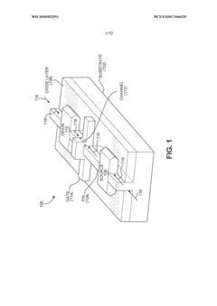
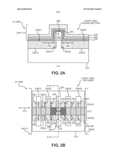
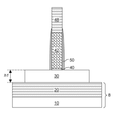
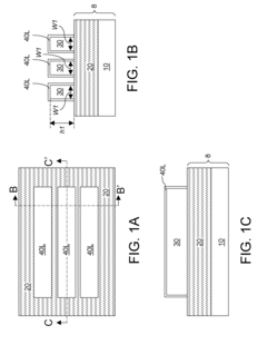
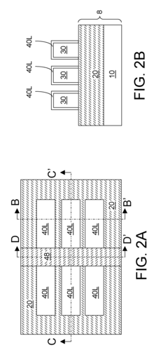
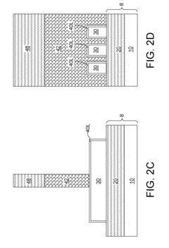
FIN field effect transistors (FETS) (finfets) employing dielectric material layers to apply stress to channel regions
PatentWO2018052591A1
Innovation
- Employing dielectric material layers on either side of the Fin to apply stress to the channel region, which provides consistent stress levels regardless of the FinFET area, unlike epitaxial layers or shallow trench isolation methods.
FinFET with longitudinal stress in a channel
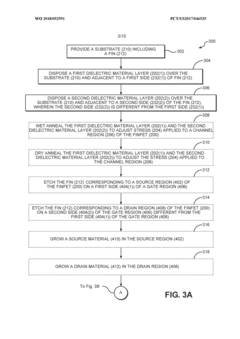
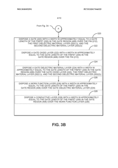
PatentActiveUS7872303B2
Innovation
- The method involves forming semiconductor fins on an insulator layer, etching the end portions to reduce their height and width, and growing lattice-mismatched semiconductor material epitaxially on these portions to apply longitudinal stress along the channel, using selective epitaxy to align the material with the fin, thereby enhancing device performance.
Standardization Efforts in Semiconductor Reliability Testing
The semiconductor industry has recognized the critical need for standardized reliability testing methodologies, particularly for advanced technologies like FinFETs operating under high-stress conditions. Several international organizations have been instrumental in developing these standards, with the Joint Electron Device Engineering Council (JEDEC) leading many initiatives specifically focused on transistor reliability testing protocols.
JEDEC's JEP122 standard provides comprehensive guidelines for determination of reliability statistics, while their JC-14.2 committee continually updates testing methodologies for emerging semiconductor technologies. These standards have evolved to address the unique challenges posed by three-dimensional FinFET structures, including specialized test patterns for hot carrier injection (HCI) and bias temperature instability (BTI) phenomena.
The International Electrotechnical Commission (IEC) has complemented these efforts through its Technical Committee 47, which focuses on semiconductor devices and has established the IEC 60749 series of standards covering environmental and endurance test methods. These standards have been adapted to incorporate testing procedures specific to high-stress conditions relevant to FinFET reliability assessment.
Semiconductor Equipment and Materials International (SEMI) has contributed significantly through its Standards Program, developing test methods that ensure consistency in reliability data collection across different manufacturing facilities. Their standards address sample preparation, measurement techniques, and data reporting formats that enable meaningful comparison of reliability results between different research groups and manufacturers.
Industry consortia like the Semiconductor Research Corporation (SRC) have facilitated collaborative efforts between academia and industry to develop standardized reliability models for FinFETs. These models incorporate acceleration factors for temperature, voltage, and frequency, allowing for more accurate lifetime predictions under various operating conditions.
Recent standardization efforts have focused on addressing the statistical challenges in reliability testing, with emphasis on sample sizes required for meaningful data collection and statistical methods for extrapolating accelerated test results to normal operating conditions. The IEEE International Reliability Physics Symposium (IRPS) has served as a forum for discussing and refining these methodologies.
Despite these advances, standardization gaps remain in quantifying reliability under extreme conditions that exceed typical operating parameters. Current efforts are addressing these gaps through round-robin testing programs where multiple laboratories test identical devices using standardized protocols, thereby validating the reproducibility of reliability measurements for FinFETs under high-stress conditions.
Economic Impact of FinFET Reliability on Semiconductor Industry
The economic implications of FinFET reliability under high-stress conditions extend far beyond technical considerations, significantly impacting the semiconductor industry's financial landscape. Reliability issues in FinFET technology directly translate to increased manufacturing costs, with defect rates in high-stress applications potentially increasing production expenses by 15-30% compared to standard operating conditions. These additional costs stem from more rigorous testing protocols, specialized equipment requirements, and higher rejection rates during quality control processes.
Market competitiveness is heavily influenced by reliability metrics, with semiconductor manufacturers that demonstrate superior FinFET performance under extreme conditions commanding premium pricing and securing contracts in high-value sectors such as aerospace, automotive, and medical devices. Industry analysis indicates that companies with proven reliability in high-stress environments typically achieve 8-12% higher profit margins compared to competitors with average reliability ratings.
The insurance and warranty costs associated with FinFET reliability present another substantial economic factor. Semiconductor companies providing components for critical applications face increasing pressure to offer extended warranties, with potential liability for downstream failures reaching hundreds of millions of dollars in extreme cases. This has prompted a 22% increase in specialized technology insurance premiums over the past five years for manufacturers serving high-reliability markets.
Investment patterns within the industry have shifted noticeably toward reliability-focused research and development. Venture capital funding for startups specializing in FinFET reliability enhancement technologies has grown at a compound annual rate of 17.3% since 2018, reflecting market recognition of reliability as a critical economic differentiator. Major semiconductor manufacturers now allocate approximately 12-15% of their R&D budgets specifically to reliability improvement initiatives.
Supply chain economics have also evolved in response to reliability concerns. Tier-one semiconductor suppliers increasingly implement stringent reliability requirements for their component providers, creating cascading economic effects throughout the supply chain. This has led to industry consolidation, with smaller firms unable to meet escalating reliability standards being acquired or exiting certain market segments entirely.
The long-term economic sustainability of semiconductor manufacturers now correlates strongly with their ability to quantify and improve FinFET reliability under high-stress conditions. Companies that have established leadership in this domain have demonstrated 23% better stock performance over the past decade compared to industry averages, highlighting how technical reliability translates directly to economic resilience and shareholder value.
Unlock deeper insights with Patsnap Eureka Quick Research — get a full tech report to explore trends and direct your research. Try now!
Generate Your Research Report Instantly with AI Agent
Supercharge your innovation with Patsnap Eureka AI Agent Platform!