How To Measure FinFET Electrical Properties Precisely
SEP 11, 20259 MIN READ
Generate Your Research Report Instantly with AI Agent
Patsnap Eureka helps you evaluate technical feasibility & market potential.
FinFET Measurement Background and Objectives
FinFET technology has revolutionized semiconductor manufacturing since its introduction in the early 2000s. The evolution from planar transistors to three-dimensional fin field-effect transistors marked a significant milestone in addressing the challenges of continuous device scaling according to Moore's Law. This transition was necessitated by the increasing short-channel effects and leakage currents that plagued traditional MOSFET designs as dimensions shrank below 22nm.
The precise measurement of FinFET electrical properties has become increasingly critical as these devices continue to scale down to 5nm and beyond. Historically, measurement techniques evolved from simple current-voltage characterization to sophisticated multi-parameter extraction methodologies that account for quantum effects and three-dimensional electron transport phenomena. The industry has witnessed a parallel development of specialized metrology tools designed specifically for FinFET structures.
Current measurement objectives focus on achieving nanometer-scale precision while maintaining high throughput for manufacturing environments. Key parameters requiring precise measurement include threshold voltage, carrier mobility, series resistance, capacitance characteristics, and reliability factors such as bias temperature instability and hot carrier effects. The unique geometry of FinFETs presents specific measurement challenges not encountered in planar devices.
Recent technological trends indicate a growing emphasis on in-line and non-destructive measurement techniques that can be integrated into production workflows. The development of scatterometry, electrical test structures, and advanced scanning probe microscopy methods has significantly contributed to improving measurement accuracy while reducing test times. Additionally, machine learning algorithms are increasingly being employed to enhance measurement precision and extract meaningful patterns from complex datasets.
The ultimate technical goal is to develop measurement methodologies capable of accurately characterizing sub-nanometer variations in electrical properties across billions of transistors on a single chip. This requires overcoming fundamental physical limitations related to quantum effects, statistical variations, and signal-to-noise ratios at extremely small scales. Furthermore, these measurements must be performed at speeds compatible with high-volume manufacturing environments.
International roadmaps such as the International Roadmap for Devices and Systems (IRDS) have established benchmarks for measurement precision that continue to drive innovation in this field. The convergence of advanced instrumentation, computational modeling, and artificial intelligence promises to deliver the next generation of measurement technologies capable of meeting the increasingly stringent requirements of future FinFET nodes and their eventual successors in the semiconductor technology continuum.
Market Demand for Precise FinFET Characterization
The semiconductor industry's demand for precise FinFET electrical characterization has experienced exponential growth since the introduction of FinFET technology in commercial production around 2011. This demand is primarily driven by the continuous miniaturization of transistors, with leading manufacturers now producing chips at 3nm and 2nm nodes, where precise electrical measurements become critical for both development and production.
Market research indicates that the semiconductor test equipment market specifically for advanced node characterization exceeded $5.7 billion in 2022, with a compound annual growth rate of approximately 6.8%. Within this segment, equipment dedicated to FinFET electrical property measurement represents a significant and growing portion, estimated at $1.2 billion annually.
The primary market drivers stem from several industry imperatives. Firstly, yield optimization remains paramount as manufacturers struggle with decreasing yields at advanced nodes. Precise electrical characterization enables early identification of process variations and defects, directly impacting production economics. Industry reports suggest that a 1% yield improvement at advanced nodes can translate to millions in additional revenue.
Secondly, the increasing complexity of chip designs incorporating heterogeneous integration demands more sophisticated measurement capabilities. Multi-gate architectures, gate-all-around FETs, and vertical stacking create new measurement challenges that conventional techniques cannot adequately address.
The automotive and high-reliability markets represent another significant demand vector. As FinFETs increasingly power safety-critical systems in autonomous vehicles and medical devices, reliability characterization requirements have intensified, with automotive-grade semiconductors requiring comprehensive electrical parameter verification across extended temperature and voltage ranges.
Geographically, the demand is concentrated in regions with advanced semiconductor manufacturing capabilities. East Asia (particularly Taiwan, South Korea, and Japan) accounts for approximately 65% of the market, followed by North America at 22% and Europe at 10%.
Key customer segments include integrated device manufacturers (IDMs), foundries, fabless semiconductor companies, and research institutions. Foundries represent the largest market segment, accounting for approximately 40% of demand, as they require precise characterization tools to develop and maintain competitive process technologies.
Looking forward, market analysts project continued strong growth in this sector, driven by the transition to gate-all-around FETs and eventual 3D vertical architectures, which will further increase measurement complexity and precision requirements. The emergence of quantum computing and neuromorphic computing applications is also expected to create new specialized measurement needs for novel device structures.
Current Challenges in FinFET Electrical Measurement
Despite significant advancements in FinFET technology, precise electrical measurement of these three-dimensional transistor structures presents numerous challenges that impede both research progress and manufacturing quality control. The non-planar geometry of FinFETs introduces fundamental difficulties in accessing and probing the active channel regions without disrupting device performance or introducing measurement artifacts.
Contact resistance characterization remains particularly problematic, as the reduced contact area between measurement probes and the fin structure creates significant variability in resistance measurements. This variability can mask the intrinsic electrical properties researchers aim to quantify, leading to inconsistent data interpretation across different measurement sessions or equipment setups.
Parasitic capacitance effects further complicate accurate measurements, especially at high frequencies. The three-dimensional structure creates complex capacitive coupling between the gate, source, drain, and substrate that conventional measurement techniques struggle to decouple. These parasitic elements significantly impact dynamic performance metrics and switching characteristics, yet isolating their contributions remains challenging.
Temperature-dependent measurements face additional hurdles, as the thermal profile across the fin structure is non-uniform and difficult to control precisely. This thermal gradient affects carrier mobility and threshold voltage measurements, introducing another layer of uncertainty in electrical characterization efforts.
The ultra-thin body and fin dimensions of advanced FinFET nodes (below 7nm) have pushed conventional measurement techniques to their physical limits. Quantum effects become increasingly prominent at these scales, requiring measurement approaches that can account for quantum confinement and tunneling phenomena that traditional bulk semiconductor models fail to capture adequately.
Statistical variability presents another significant challenge, as process variations in fin width, height, and gate length create device-to-device differences that must be characterized across large sample populations. This necessitates high-throughput measurement techniques that maintain precision while accommodating the statistical nature of advanced semiconductor manufacturing.
Reliability testing faces particular difficulties, as accelerated aging tests must accurately capture degradation mechanisms unique to FinFET structures, including hot carrier injection at fin corners and bias temperature instability effects that manifest differently than in planar devices. Current measurement protocols often fail to isolate these specific degradation modes.
Finally, the integration of new materials in advanced FinFET nodes, including high-k dielectrics and metal gates with work function engineering, introduces additional measurement complexities. Interface traps, fixed charges, and material defects at these novel interfaces require specialized characterization techniques that can distinguish between bulk and interface phenomena.
State-of-the-Art FinFET Electrical Characterization Methods
01 FinFET structure and electrical performance
The structure of FinFETs significantly impacts their electrical properties. The fin height, width, and shape determine channel control and current flow. Multi-fin structures can enhance drive current while maintaining good electrostatic control. The three-dimensional nature of FinFETs allows for better channel control compared to planar transistors, resulting in reduced short-channel effects and improved electrical characteristics such as subthreshold swing and drain-induced barrier lowering.- FinFET structure and electrical performance: The fundamental structure of FinFETs significantly impacts their electrical properties. The fin height, width, and shape determine channel control and current flow characteristics. Multi-fin designs can enhance drive current capabilities while maintaining good electrostatic control. The three-dimensional structure of FinFETs allows for better suppression of short-channel effects compared to planar transistors, resulting in improved subthreshold swing and reduced leakage current.
- Gate engineering for FinFET optimization: Gate engineering plays a crucial role in optimizing FinFET electrical properties. Various gate materials, including high-k dielectrics and metal gates, can be employed to achieve desired threshold voltages and reduce gate leakage. Gate length scaling affects performance metrics such as transconductance and on/off current ratios. Advanced gate structures like multi-gate configurations can further enhance channel control and improve carrier mobility in the fin channel.
- Doping profiles and carrier mobility enhancement: Doping concentration and distribution in FinFETs significantly influence their electrical properties. Carefully engineered doping profiles can optimize threshold voltage, reduce random dopant fluctuation effects, and minimize junction leakage. Various techniques for enhancing carrier mobility, such as channel strain engineering and material selection, can improve current drive capabilities. The relationship between doping levels and electrostatic control presents important trade-offs in FinFET design.
- FinFET scaling and performance enhancement techniques: As FinFETs scale to smaller dimensions, various techniques are employed to maintain or enhance electrical performance. These include fin pitch scaling, source/drain engineering, and contact resistance reduction methods. Advanced materials and process technologies help address challenges like parasitic capacitance and resistance that become more prominent at smaller nodes. Novel architectures such as stacked fins or complementary FET structures can provide pathways for continued performance scaling.
- Modeling and simulation of FinFET electrical characteristics: Accurate modeling and simulation techniques are essential for predicting and optimizing FinFET electrical properties. Compact models that capture the three-dimensional electrostatics and quantum effects in FinFETs enable efficient circuit design. Advanced simulation methodologies help analyze performance parameters such as on-current, off-current, subthreshold slope, and drain-induced barrier lowering. These models also facilitate the exploration of reliability issues and performance variability in FinFET technologies.
02 Gate engineering for FinFET performance optimization
Gate engineering plays a crucial role in optimizing FinFET electrical properties. This includes gate material selection, gate stack engineering, and work function tuning to achieve desired threshold voltages. Advanced gate structures such as high-k metal gates improve electrostatic control and reduce leakage current. Gate length scaling affects performance metrics like on-current, off-current ratio, and switching speed. Proper gate engineering helps balance performance requirements with power consumption constraints.Expand Specific Solutions03 Channel doping and strain engineering
Channel doping profiles and strain engineering techniques significantly influence FinFET electrical properties. Controlled doping can adjust threshold voltage and improve carrier mobility. Strain engineering, through materials like SiGe or process techniques, enhances carrier transport properties in the channel. These approaches can be combined to optimize performance metrics such as transconductance and drive current while maintaining good electrostatic control and minimizing short-channel effects.Expand Specific Solutions04 Source/drain engineering and contact resistance
Source and drain engineering significantly impacts FinFET electrical performance. Techniques include epitaxial growth of source/drain regions, selective doping, and formation of low-resistance contacts. Reducing parasitic resistance at source/drain contacts improves current drive capability and switching speed. Advanced source/drain structures can incorporate strain to enhance carrier mobility. These engineering approaches are critical for maintaining performance advantages as FinFET dimensions continue to scale down.Expand Specific Solutions05 FinFET modeling and simulation for electrical characterization
Accurate modeling and simulation techniques are essential for predicting and optimizing FinFET electrical properties. These include TCAD simulations, compact modeling, and physics-based approaches that account for quantum effects and three-dimensional electrostatics. Advanced models incorporate parameters for fin geometry, gate stack properties, and channel engineering to predict performance metrics like threshold voltage, subthreshold slope, and on/off current ratios. These tools enable efficient device design and optimization before physical fabrication.Expand Specific Solutions
Key Players in Semiconductor Measurement Equipment
The FinFET electrical property measurement market is currently in a growth phase, driven by increasing demand for precise characterization of advanced semiconductor devices. The market size is expanding rapidly as semiconductor manufacturing shifts toward sub-10nm nodes, with projections indicating significant growth through 2030. Technologically, the field is moderately mature but continuously evolving, with leading players developing increasingly sophisticated measurement solutions. TSMC, Samsung, and GlobalFoundries lead commercial implementation, while research institutions like IMEC and Chinese entities (SMIC, Huali) are advancing measurement techniques. Equipment providers KLA and Agilent Technologies offer critical metrology tools, collaborating with IBM and Qualcomm to develop next-generation measurement standards for emerging FinFET architectures.
Taiwan Semiconductor Manufacturing Co., Ltd.
Technical Solution: TSMC has developed a comprehensive suite of electrical characterization techniques for FinFET devices. Their approach combines conventional I-V and C-V measurements with advanced techniques like RF characterization and noise analysis. TSMC employs a multi-frequency capacitance measurement methodology that allows for accurate extraction of parasitic capacitances in FinFET structures, crucial for understanding device performance at the nanoscale. They have pioneered the use of scanning microwave impedance microscopy (sMIM) for non-destructive characterization of FinFET electrical properties with nanometer resolution. TSMC's methodology includes specialized test structures designed specifically for isolating and measuring individual FinFET parameters, enabling precise extraction of channel resistance, source/drain resistances, and contact resistances. Their measurement protocols incorporate temperature-dependent characterization (from -40°C to 125°C) to evaluate device reliability and performance stability across operating conditions.
Strengths: Industry-leading metrology infrastructure with nanometer-scale precision; proprietary algorithms for parasitic deembedding; comprehensive statistical analysis capabilities for process variation monitoring. Weaknesses: Highly specialized equipment requirements; complex calibration procedures needed for consistent measurements across different tool sets.
Samsung Electronics Co., Ltd.
Technical Solution: Samsung has developed an integrated electrical measurement platform specifically optimized for FinFET characterization across multiple technology nodes. Their methodology employs ultra-low-noise measurement systems capable of detecting sub-picoampere current levels, essential for accurate off-state leakage characterization in advanced FinFET devices. Samsung utilizes a proprietary multi-frequency capacitance profiling technique that enables extraction of doping profiles and interface trap densities with depth resolution below 1nm. A distinctive aspect of Samsung's approach is their implementation of on-chip measurement circuits that allow for in-situ characterization of FinFET parameters during actual circuit operation, providing insights into dynamic behavior not accessible through conventional probe-based measurements. Their platform incorporates specialized RF characterization techniques operating up to 110GHz to evaluate high-frequency performance parameters critical for communications applications. Samsung has also developed custom algorithms for separating intrinsic device parameters from parasitic elements, allowing for more accurate extraction of fundamental FinFET electrical properties across varying fin geometries and process conditions.
Strengths: Comprehensive characterization capabilities spanning DC to mmWave frequencies; advanced automation systems enabling high-throughput measurements; sophisticated data analytics for process optimization. Weaknesses: Proprietary nature of some measurement techniques limits cross-platform validation; complex calibration requirements for high-frequency measurements.
Critical Patents and Literature on FinFET Measurement
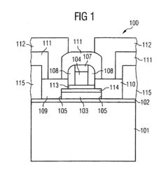
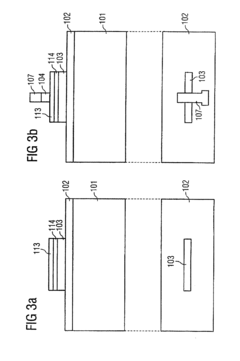
Fin Field-Effect Transistor and Method for Fabricating a Fin Field-Effect Transistor
PatentInactiveUS20080035997A1
Innovation
- A fin field-effect transistor design with self-aligned source and drain regions formed independently of the gate, using metallic conductivity materials like platinum silicide and erbium silicide, and incorporating diffusion barriers to prevent dopant indiffusion, allowing for precise doping and avoiding overlap between the gate and source/drain regions.


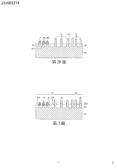
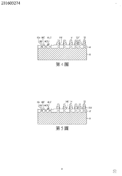
Fin field effect transistor and method of manufacturing the same
PatentActiveTW201603274A
Innovation
- A FinFET manufacturing method involving the formation of separated epitaxial layers on recessed fins with a specific insulator profile, preventing epi crystal and silicide merging, and enhancing electrical performance.

Quantum Effects in Advanced FinFET Measurements
As FinFET technology continues to scale down to sub-10nm nodes, quantum mechanical effects become increasingly significant in device operation and measurement. These quantum effects manifest primarily through electron wave-like behavior, tunneling phenomena, and quantized energy states, fundamentally altering how electrical properties must be measured and interpreted.
Quantum confinement effects in the narrow fin structure create discrete energy levels that influence carrier transport mechanisms. When measuring electrical properties such as threshold voltage and mobility, these quantized states can cause deviations from classical semiconductor physics models. Particularly in ultra-thin body FinFETs, the quantum confinement leads to bandgap widening and effective mass modification, requiring adjustments to traditional measurement methodologies.
Tunneling-related phenomena present another measurement challenge. Direct source-to-drain tunneling and gate-induced drain leakage (GIDL) enhanced by band-to-band tunneling can significantly impact subthreshold characteristics. These quantum tunneling effects necessitate specialized measurement techniques that can differentiate between classical drift-diffusion current and quantum tunneling components.
Temperature dependence of quantum effects adds another layer of complexity. While classical semiconductor behavior typically shows predictable temperature scaling, quantum effects often exhibit non-linear temperature dependencies. Measurement protocols must therefore incorporate temperature variation studies to properly characterize these quantum-influenced parameters.
Advanced measurement techniques addressing these quantum effects include low-temperature characterization systems capable of operating near liquid helium temperatures, where quantum behaviors become more pronounced and separable from thermal effects. Scanning tunneling microscopy and spectroscopy (STM/STS) techniques provide spatial resolution of quantum states within the FinFET structure, offering insights into local variations in quantum confinement.
Capacitance-voltage (C-V) measurements at multiple frequencies have proven valuable for extracting quantum capacitance effects, which directly relate to the density of states modified by quantum confinement. These measurements, when performed with precision high-frequency instruments, can reveal subtle quantum mechanical influences on carrier distribution.
Modeling and simulation tools have evolved to incorporate quantum corrections, enabling more accurate interpretation of measurement data. Density functional theory (DFT) calculations, non-equilibrium Green's function (NEGF) methods, and quantum-corrected Monte Carlo simulations now serve as essential companions to experimental measurements, helping to deconvolve quantum effects from measured electrical parameters.
Standardization Efforts for FinFET Electrical Testing
The standardization of FinFET electrical testing methodologies has become increasingly critical as semiconductor manufacturing advances into sub-10nm nodes. Industry bodies such as IEEE, JEDEC, and SEMI have been actively developing comprehensive standards to ensure consistency and reliability in FinFET characterization across the semiconductor ecosystem.
IEEE's P2427 working group has established significant protocols specifically addressing FinFET electrical parameter extraction, focusing on standardizing measurement conditions for key parameters including threshold voltage, carrier mobility, and parasitic capacitance. These standards define precise temperature ranges, voltage sweep rates, and measurement frequencies to minimize variability between testing facilities.
JEDEC has complemented these efforts through its JC-14.2 committee, which has published guidelines for FinFET reliability testing, emphasizing standardized approaches to bias temperature instability (BTI) and hot carrier injection (HCI) measurements. Their JESD92 document series provides detailed procedures for stress conditions and recovery measurements that are particularly relevant to three-dimensional transistor architectures.
The International Roadmap for Devices and Systems (IRDS), successor to ITRS, has established metrology benchmarks specifically for advanced transistor structures, including recommended equipment specifications and calibration procedures for accurate FinFET electrical characterization. These recommendations have been widely adopted by equipment manufacturers and testing laboratories.
Semiconductor manufacturers have also contributed to standardization through industry consortia like imec and SEMATECH, developing reference test structures and measurement methodologies. The Global Semiconductor Alliance (GSA) has facilitated cross-company working groups to harmonize testing approaches, particularly for process development and quality control applications.
Equipment manufacturers have responded by developing calibration standards and reference materials specifically designed for FinFET testing. Companies like Keysight Technologies and Advantest have created verification protocols that ensure measurement systems meet the precision requirements outlined in industry standards, with traceability to national metrology institutes.
The standardization landscape continues to evolve with the emergence of new FinFET variants and gate-all-around architectures. Current efforts are focusing on extending existing standards to accommodate multi-gate configurations, ultra-thin body dimensions, and the integration of new channel materials like silicon-germanium and III-V compounds, ensuring that measurement methodologies remain relevant as technology advances.
Unlock deeper insights with Patsnap Eureka Quick Research — get a full tech report to explore trends and direct your research. Try now!
Generate Your Research Report Instantly with AI Agent
Supercharge your innovation with Patsnap Eureka AI Agent Platform!