How To Reduce Leakage Current In FinFET Devices
SEP 11, 20259 MIN READ
Generate Your Research Report Instantly with AI Agent
Patsnap Eureka helps you evaluate technical feasibility & market potential.
FinFET Leakage Current Background and Objectives
FinFET technology emerged as a revolutionary advancement in semiconductor manufacturing, addressing the limitations of planar MOSFET designs as device dimensions continued to shrink below 22nm. Since their commercial introduction in the early 2010s, FinFETs have become the cornerstone of modern high-performance computing due to their superior electrostatic control and reduced short-channel effects. However, as scaling continues toward 5nm and beyond, leakage current has emerged as a critical challenge threatening the power efficiency and reliability of these devices.
The evolution of FinFET technology has been marked by continuous refinements aimed at balancing performance enhancement with power consumption reduction. Initial implementations focused primarily on structural optimization, while recent developments have increasingly emphasized material innovations and novel gate engineering techniques to combat leakage mechanisms. Industry roadmaps suggest that managing leakage current will be pivotal for extending FinFET viability before potential transitions to gate-all-around or nanosheet architectures.
Leakage current in FinFETs manifests through multiple mechanisms, including subthreshold leakage, gate leakage, and band-to-band tunneling. These phenomena have become more pronounced with each technology node shrink, as thinner gate oxides and reduced channel lengths exacerbate quantum mechanical effects. The semiconductor industry has established that a comprehensive understanding of these leakage pathways is essential for developing effective mitigation strategies.
The primary technical objective of this investigation is to identify and evaluate cutting-edge approaches for reducing leakage current in FinFET devices while maintaining or improving performance metrics. Specifically, we aim to explore solutions that can achieve at least a 30% reduction in static power consumption compared to current-generation FinFETs without compromising switching speed or area efficiency.
Secondary objectives include assessing the manufacturability and cost implications of proposed leakage reduction techniques, determining their compatibility with existing fabrication infrastructure, and evaluating their scalability for future technology nodes. Additionally, we seek to establish quantitative benchmarks for leakage current optimization that can guide future research and development efforts.
This technical exploration will encompass both incremental improvements to established FinFET architectures and potentially disruptive innovations that could fundamentally alter the leakage current profile. By comprehensively examining the technological landscape, we intend to chart a clear path forward for sustaining Moore's Law scaling through enhanced FinFET designs with dramatically improved power efficiency.
Market Demand for Low-Power FinFET Solutions
The global semiconductor market has witnessed a significant shift towards low-power solutions, with FinFET technology emerging as a critical component in this transition. Market research indicates that power consumption has become a primary concern for semiconductor manufacturers, particularly as mobile devices, IoT applications, and data centers continue to proliferate worldwide.
The demand for low-power FinFET solutions is primarily driven by the mobile device sector, where battery life remains a crucial differentiating factor for consumers. Smartphone manufacturers are increasingly seeking semiconductor components that can deliver high performance while minimizing power consumption, creating a substantial market opportunity for advanced FinFET technologies with reduced leakage current.
Data center operators represent another significant market segment demanding low-power FinFET solutions. With the exponential growth in cloud computing and data processing requirements, energy consumption has become both an environmental concern and a major operational cost. The reduction of leakage current in FinFET devices directly translates to lower power bills and cooling requirements for these facilities.
The automotive industry has emerged as a rapidly growing market for low-power semiconductor solutions. As vehicles incorporate more advanced driver assistance systems (ADAS) and move towards autonomous driving capabilities, the need for energy-efficient computing has intensified. FinFET devices with minimal leakage current are particularly valuable in this context, as they help extend the range of electric vehicles and reduce the overall power requirements of automotive electronics.
Consumer electronics beyond smartphones—including wearables, smart home devices, and portable computing—represent another substantial market segment. These devices often operate on limited battery capacity or energy harvesting techniques, making power efficiency a critical requirement. The market for ultra-low-power FinFET solutions in this segment is expected to grow substantially as IoT adoption accelerates globally.
Industrial applications and edge computing deployments are creating additional demand for power-efficient semiconductor solutions. These applications often operate in remote or challenging environments where power availability is limited, making leakage current reduction a valuable feature.
Market forecasts suggest that semiconductor manufacturers who can effectively address leakage current challenges in FinFET devices stand to capture significant market share across these diverse sectors. The economic value proposition is compelling: even marginal improvements in power efficiency can translate to substantial competitive advantages in the marketplace, particularly as devices continue to shrink and power density increases.
Current Challenges in FinFET Leakage Control
Despite significant advancements in FinFET technology, leakage current remains a persistent challenge that threatens to undermine the efficiency gains offered by these devices. As process nodes continue to shrink below 10nm, quantum mechanical effects become increasingly pronounced, exacerbating leakage issues. Gate leakage through tunneling mechanisms has emerged as a critical concern, with electrons able to penetrate the ultra-thin gate dielectric despite improvements in high-k materials.
Subthreshold leakage presents another major challenge, occurring when the transistor fails to completely turn off at voltages below threshold. This issue is particularly problematic in mobile and IoT applications where devices spend significant time in standby mode. The multi-gate structure of FinFETs, while improving channel control, introduces complex three-dimensional leakage paths that are difficult to model and mitigate.
Band-to-band tunneling (BTBT) leakage has become increasingly significant at advanced nodes, occurring when electrons tunnel directly from the valence band to the conduction band in high electric field regions. This phenomenon is particularly pronounced at the drain-body junction where field concentration is highest, and becomes more severe with aggressive device scaling.
Junction leakage at the source/drain interfaces represents another substantial challenge. As junction depths decrease to maintain short-channel control, the resulting higher doping concentrations create steeper electric fields that facilitate various leakage mechanisms. Additionally, the three-dimensional nature of FinFET structures complicates junction formation and increases the potential for defect-assisted leakage paths.
Temperature dependence adds another layer of complexity, as leakage currents typically increase exponentially with rising temperatures. This creates a troublesome feedback loop where initial leakage generates heat, which in turn exacerbates leakage further. Managing this thermal runaway effect becomes particularly challenging in high-performance computing applications with dense transistor integration.
Process variations and manufacturing defects significantly impact leakage characteristics, with fin width fluctuations being especially problematic. Even minor variations in fin dimensions can dramatically alter threshold voltages and subthreshold slopes, leading to unpredictable leakage behavior across a chip. This variability complicates both design and yield management.
The industry faces a fundamental power-performance tradeoff, as techniques to reduce leakage often negatively impact switching speed or drive current. Finding the optimal balance between static and dynamic power consumption while maintaining performance targets represents perhaps the most significant challenge in contemporary FinFET design and manufacturing.
Mainstream Leakage Current Mitigation Strategies
01 Gate structure modifications to reduce leakage current
Various gate structure modifications can be implemented in FinFET devices to reduce leakage current. These include using high-k gate dielectric materials, metal gate electrodes, and optimized gate stack configurations. By engineering the gate structure with appropriate materials and dimensions, the gate-to-channel leakage can be minimized, resulting in improved device performance and power efficiency.- Gate structure modifications to reduce leakage current: Various modifications to the gate structure of FinFET devices can significantly reduce leakage current. These include using high-k gate dielectric materials, metal gate electrodes, and optimized gate length designs. Gate engineering techniques such as work function tuning and gate stack optimization help control threshold voltage and minimize gate-induced drain leakage (GIDL), resulting in improved device performance and power efficiency.
- Source/drain engineering for leakage reduction: Engineering the source and drain regions of FinFET devices plays a crucial role in reducing leakage current. Techniques include epitaxial growth of strained materials, optimized doping profiles, and formation of extended source/drain regions. Implementation of lightly doped drain (LDD) structures and careful junction design helps minimize junction leakage and short-channel effects, contributing to overall lower power consumption in FinFET devices.
- Channel engineering techniques: Channel engineering techniques are employed to control leakage current in FinFET devices. These include fin width optimization, channel doping concentration adjustments, and implementation of multi-threshold voltage designs. Introduction of strain in the channel region and use of alternative channel materials can enhance carrier mobility while suppressing leakage paths. These approaches help maintain the balance between performance and power consumption in advanced FinFET technologies.
- Multi-fin and 3D integration approaches: Advanced multi-fin and three-dimensional integration approaches are utilized to address leakage current challenges in FinFET devices. These include optimized fin spacing, fin height control, and implementation of stacked fin structures. Novel 3D integration techniques allow for better electrostatic control and reduced parasitic effects, resulting in minimized leakage paths and improved power efficiency in high-density integrated circuits.
- Biasing and circuit-level techniques: Biasing and circuit-level techniques provide effective methods for managing leakage current in FinFET-based designs. These include adaptive body biasing, power gating strategies, and implementation of multi-threshold voltage circuit designs. Dynamic voltage scaling and leakage-aware circuit optimization techniques help minimize standby power consumption while maintaining performance requirements during active operation modes.
02 Source/drain engineering techniques
Engineering the source and drain regions of FinFET devices can significantly reduce leakage current. Techniques include optimizing doping profiles, implementing epitaxial growth of source/drain regions, and creating strain in these regions. These modifications help control junction leakage and improve carrier mobility, resulting in reduced off-state current and better overall device performance.Expand Specific Solutions03 Channel design and optimization
The design and optimization of the FinFET channel plays a crucial role in controlling leakage current. This includes adjusting the fin width and height, implementing multi-fin structures, and optimizing channel doping. By carefully engineering the channel dimensions and material properties, short-channel effects can be suppressed, resulting in reduced subthreshold leakage current.Expand Specific Solutions04 Threshold voltage control methods
Various methods can be employed to control the threshold voltage of FinFET devices, which directly impacts leakage current. These include work function engineering of gate materials, channel doping adjustments, and implementation of multiple threshold voltage designs. By optimizing the threshold voltage, the off-state leakage current can be minimized while maintaining the required on-state performance.Expand Specific Solutions05 Advanced isolation techniques
Implementing advanced isolation techniques in FinFET devices helps minimize leakage paths between adjacent transistors and regions. These techniques include optimized shallow trench isolation (STI), fin isolation structures, and punch-through stoppers. By effectively isolating the active regions of the device, parasitic leakage currents can be significantly reduced, improving the overall power efficiency of the FinFET.Expand Specific Solutions
Key Industry Players in FinFET Technology
The FinFET leakage current reduction landscape is currently in a mature development phase, with the market expanding as advanced node technologies proliferate. Leading players Taiwan Semiconductor Manufacturing Co. (TSMC) and Samsung Electronics dominate with advanced process technologies, while companies like Intel, Qualcomm, and IBM contribute significant innovations. The competitive field includes foundries like United Microelectronics Corp. (UMC) and Semiconductor Manufacturing International Corporation (SMIC) working to close the technology gap. Research institutions including Tufts University and the Institute of Microelectronics of Chinese Academy of Sciences collaborate with industry to address fundamental challenges. The technology has reached commercial maturity at 7nm and below nodes, with ongoing research focused on sub-3nm architectures and novel materials to further mitigate quantum tunneling effects and reduce static power consumption.
Taiwan Semiconductor Manufacturing Co., Ltd.
Technical Solution: TSMC has pioneered multiple innovative approaches to reduce leakage current in FinFET devices. Their primary strategy involves implementing multi-Vt (threshold voltage) design techniques, where they offer different transistor options with varying threshold voltages to balance performance and leakage. TSMC's N5 and N3 process nodes incorporate high-k metal gate (HKMG) technology with optimized gate stack materials that minimize gate leakage by up to 90% compared to conventional SiO2 dielectrics[1]. They've also developed strain engineering techniques that enhance carrier mobility while simultaneously reducing leakage paths. TSMC implements source/drain engineering with epitaxial growth of SiGe for PMOS and Si:C for NMOS to create favorable band alignments that suppress leakage mechanisms. Additionally, their advanced FinFET designs feature optimized fin geometry with precise height-to-width ratios that maximize electrostatic control while minimizing short-channel effects that contribute to leakage[3].
Strengths: Industry-leading process technology with exceptional gate control and electrostatic properties; comprehensive multi-Vt offerings allowing designers to optimize power-performance tradeoffs; mature manufacturing capabilities ensuring high yield and reliability. Weaknesses: Their advanced solutions often require sophisticated design tools and methodologies, increasing complexity for chip designers; premium pricing compared to less advanced nodes.
Semiconductor Manufacturing International (Shanghai) Corp.
Technical Solution: SMIC has developed a multi-faceted approach to reduce leakage current in their FinFET technology nodes. Their strategy focuses on practical implementations suitable for their manufacturing capabilities. SMIC employs optimized gate stack engineering with carefully selected high-k dielectric materials and metal gates that reduce gate leakage while maintaining reliability. Their FinFET process incorporates multi-Vt options through work function metal engineering, allowing designers to select appropriate threshold voltages for different circuit blocks based on performance and leakage requirements. SMIC has implemented advanced fin formation techniques with precise control of fin width and height to optimize the electrostatic control of the channel. They utilize source-drain engineering with optimized epitaxial growth processes and doping profiles to reduce junction leakage. Additionally, SMIC employs punch-through stopper implants beneath the channel to minimize sub-threshold leakage without degrading carrier mobility. Their process also features optimized spacer design and materials to control short-channel effects that contribute to leakage current[8]. SMIC continues to refine their FinFET technology to improve leakage characteristics while maintaining competitive manufacturing costs.
Strengths: Cost-effective implementation of leakage reduction techniques suitable for mainstream applications; growing expertise in FinFET manufacturing; ability to customize processes for specific customer requirements. Weaknesses: Technology generally trails industry leaders by 1-2 generations; more limited options in advanced materials and structures compared to leading foundries; subject to certain technology access restrictions due to geopolitical factors.
Critical Patents and Research on FinFET Leakage Reduction
Semiconductor device and manufacturing method thereof
PatentActiveUS20210376115A1
Innovation
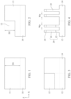
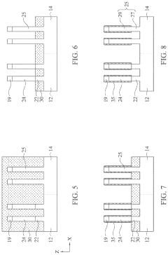
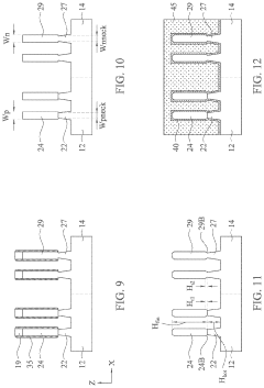
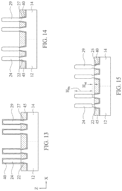
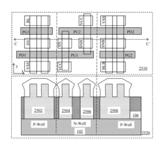
- The manufacturing process involves forming fin structures with a bottom part and an upper part over a substrate, where the bottom part is trimmed to have a smaller width than the upper part, and an isolation insulating layer is formed to expose the upper part, allowing for the formation of a dummy gate structure and source/drain structures, which are then replaced with metal gate structures, effectively covering the neck portion with a gate dielectric layer.
Apparatus for FinFETs
PatentActiveUS20160293604A1
Innovation
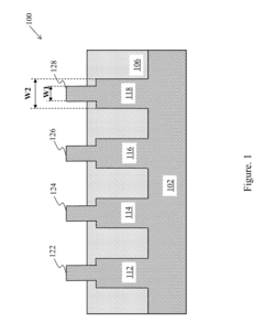
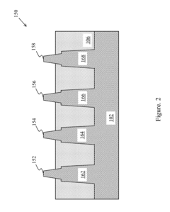
- The development of FinFETs with a reverse T-shaped channel region, where the active region protrudes from the semiconductor substrate and the gate structure wraps around three sides, enhancing control over the channel and reducing leakage current.
Thermal Management Impact on FinFET Leakage
Thermal management has emerged as a critical factor in controlling leakage current in FinFET devices. As transistor dimensions continue to shrink below 10nm, the power density increases dramatically, leading to significant thermal challenges. The relationship between temperature and leakage current follows an exponential pattern, with studies indicating that leakage current approximately doubles for every 10°C increase in temperature for advanced FinFET nodes.
Device self-heating effects are particularly pronounced in FinFET architectures due to their three-dimensional structure and reduced thermal conductivity paths. The fin geometry, while beneficial for electrostatic control, creates thermal bottlenecks that impede efficient heat dissipation. Measurements have shown that the effective temperature within the channel region can be 15-20°C higher than the substrate temperature during high-performance operation.
Advanced cooling solutions have demonstrated significant impact on reducing leakage current. Implementation of microfluidic cooling channels integrated within the chip package has shown potential to reduce junction temperatures by up to 30°C, resulting in leakage current reduction of approximately 75% compared to conventional air cooling methods. These solutions, however, introduce additional manufacturing complexity and reliability concerns.
Dynamic thermal management (DTM) techniques offer another approach to mitigating temperature-induced leakage. Adaptive voltage scaling and frequency throttling based on real-time thermal sensing have proven effective in maintaining thermal equilibrium. Recent research indicates that predictive DTM algorithms utilizing machine learning can anticipate thermal hotspots before they form, reducing average leakage power by 18-22% compared to reactive approaches.
Material innovations also play a crucial role in thermal management for leakage reduction. High thermal conductivity substrates, such as silicon-on-diamond (SoD) and silicon-on-sapphire (SoS), have demonstrated thermal resistance improvements of up to 40% compared to conventional silicon substrates. Additionally, novel gate stack materials with lower thermal resistance are being explored to facilitate more efficient heat extraction from the channel region.
The integration of thermal-aware design methodologies at both circuit and system levels has become essential. Thermal-aware placement and routing algorithms that consider heat distribution across the die have shown the ability to reduce peak temperatures by 8-12°C, translating to approximately 30% reduction in leakage power. Furthermore, thermally-optimized standard cell libraries that incorporate heat dissipation characteristics into the design process are gaining traction in advanced node designs.
Manufacturing Process Optimization for Leakage Control
Manufacturing process optimization represents a critical frontier in addressing leakage current challenges in FinFET devices. The fabrication precision directly impacts device performance, with even nanometer-scale variations potentially causing significant leakage pathways. Current manufacturing processes must evolve to accommodate increasingly stringent requirements for sub-7nm nodes where quantum effects become more pronounced.
High-k metal gate (HKMG) process refinement offers substantial leakage reduction potential. By optimizing atomic layer deposition (ALD) parameters, manufacturers can achieve more uniform gate dielectric layers with fewer defects. Recent advancements in ALD technology have demonstrated up to 30% reduction in gate leakage when deposition temperatures and precursor exposure times are precisely controlled.
Source/drain engineering presents another optimization avenue. Advanced epitaxial growth techniques for SiGe source/drain regions can reduce band-to-band tunneling leakage by creating favorable band alignments. Implementing optimized annealing processes after implantation helps minimize defect-induced junction leakage while maintaining desired dopant profiles.
Channel surface treatment before gate stack formation significantly impacts interface quality. Hydrogen annealing and nitrogen plasma treatments have shown effectiveness in passivating dangling bonds at the silicon-oxide interface, reducing interface trap density by up to 40% in recent studies. These treatments must be carefully integrated into the process flow to avoid disrupting subsequent fabrication steps.
Fin profile control represents perhaps the most critical manufacturing challenge. Achieving vertical, uniform fins with minimal line edge roughness requires advanced lithography and etching techniques. Multi-patterning approaches combined with selective deposition methods have demonstrated improved fin uniformity, directly correlating with reduced leakage variability across wafers.
Post-etching treatments to repair lattice damage have emerged as essential process steps. Hydrogen annealing at precisely controlled temperatures can heal crystal defects while maintaining fin dimensions. Similarly, advanced spacer formation techniques using conformal ALD processes help prevent parasitic leakage paths between gate and source/drain regions.
Statistical process control methodologies must evolve to detect subtle variations that impact leakage. Advanced metrology techniques including in-line electrical testing and machine learning algorithms can identify process drift before it manifests as increased leakage in finished devices. These approaches enable real-time process adjustments that maintain optimal manufacturing conditions throughout high-volume production.
Unlock deeper insights with Patsnap Eureka Quick Research — get a full tech report to explore trends and direct your research. Try now!
Generate Your Research Report Instantly with AI Agent
Supercharge your innovation with Patsnap Eureka AI Agent Platform!