FinFET Performance Benchmark: Signal Integrity Tests
SEP 11, 20259 MIN READ
Generate Your Research Report Instantly with AI Agent
PatSnap Eureka helps you evaluate technical feasibility & market potential.
FinFET Technology Evolution and Objectives
FinFET technology has evolved significantly since its introduction in the early 2000s, transforming the semiconductor industry by addressing the limitations of traditional planar transistors. Initially developed to combat short-channel effects that emerged as transistor dimensions shrank below 28nm, FinFET architecture introduced a three-dimensional fin-like structure that allowed for better electrostatic control of the channel. This revolutionary design enabled continued scaling according to Moore's Law when conventional approaches reached their physical limits.
The evolution of FinFET technology can be traced through several key generations. First-generation FinFETs, introduced at the 22nm node, demonstrated improved performance with reduced leakage current compared to planar transistors. Second-generation FinFETs at 14/16nm nodes featured refined fin structures with enhanced carrier mobility. Third-generation implementations at 10/7nm incorporated additional innovations such as strain engineering and contact resistance reduction techniques to further boost performance.
Signal integrity has become increasingly critical throughout this evolution, particularly as operating frequencies increased and supply voltages decreased. Early FinFET designs faced challenges with parasitic capacitance and resistance that could compromise signal integrity in high-speed applications. Subsequent generations have progressively addressed these issues through innovations in fin geometry, gate stack engineering, and interconnect design.
The primary objectives of current FinFET technology development, particularly regarding signal integrity testing, focus on several key areas. First is the minimization of parasitic elements that can degrade signal quality, especially in high-frequency applications where even small capacitive or inductive effects can significantly impact performance. Second is the reduction of noise coupling between adjacent components, which becomes more pronounced as device density increases.
Another critical objective is improving electromigration resistance to ensure long-term reliability under high-current conditions. As current densities increase with each technology node, ensuring robust signal integrity over the device lifetime becomes increasingly challenging. Additionally, developers aim to enhance ESD protection capabilities while maintaining performance, as the reduced dimensions of advanced FinFETs make them inherently more susceptible to electrostatic damage.
Looking forward, the technology roadmap for FinFETs includes further refinements in fin geometry, gate materials, and contact engineering to support operation at higher frequencies with improved signal integrity. The ultimate goal is to enable the next generation of high-performance computing applications, from artificial intelligence accelerators to advanced wireless communication systems, where signal integrity is paramount for achieving the desired performance and reliability targets.
Market Demand for High-Performance Signal Integrity
The signal integrity market is experiencing robust growth driven by the increasing complexity of semiconductor devices, particularly in FinFET technology. As transistor dimensions continue to shrink below 10nm, signal integrity has become a critical factor in determining overall system performance and reliability. The global market for signal integrity solutions is projected to reach $2.7 billion by 2025, growing at a CAGR of 8.3% from 2020, according to recent industry analyses.
This growth is primarily fueled by the expanding telecommunications sector, the proliferation of data centers, and the increasing adoption of high-speed interfaces in consumer electronics. With the rollout of 5G networks worldwide, there is an unprecedented demand for high-performance signal integrity solutions that can handle multi-gigabit data rates while maintaining signal quality and minimizing interference.
The automotive industry represents another significant market driver, as modern vehicles incorporate increasingly sophisticated electronic systems requiring robust signal integrity. Advanced driver-assistance systems (ADAS) and autonomous driving technologies demand ultra-reliable signal processing capabilities where even minor signal degradation could have serious consequences.
From an end-user perspective, there is a growing need for signal integrity solutions that address power consumption concerns. As mobile devices and IoT applications continue to proliferate, manufacturers are seeking signal integrity technologies that maintain performance while minimizing energy usage. This has led to increased interest in FinFET-based solutions, which offer superior performance-per-watt characteristics compared to traditional MOSFET designs.
Enterprise customers, particularly in cloud computing and high-performance computing sectors, are driving demand for signal integrity solutions capable of supporting ever-increasing data rates. These customers require technologies that can maintain signal quality across longer transmission distances and through multiple connection points, creating opportunities for advanced signal integrity testing and validation tools.
Geographically, Asia-Pacific represents the fastest-growing market for signal integrity solutions, with China, Taiwan, and South Korea leading the charge due to their dominant positions in semiconductor manufacturing. North America remains a significant market, driven by research institutions and technology companies focused on pushing the boundaries of semiconductor performance.
The market is also seeing increased demand for integrated signal integrity solutions that combine hardware and software components to provide comprehensive analysis and optimization capabilities. This trend reflects the growing complexity of modern electronic systems and the need for holistic approaches to signal integrity management.
Current FinFET Signal Integrity Challenges
Signal integrity challenges in FinFET technology have become increasingly critical as semiconductor devices continue to scale down to sub-10nm nodes. The three-dimensional fin structure, while offering superior electrostatic control and reduced short-channel effects, introduces complex signal integrity issues that were less prominent in planar MOSFET designs. These challenges directly impact circuit performance, reliability, and power consumption in advanced integrated circuits.
One of the primary signal integrity challenges in current FinFET technology is the increased parasitic capacitance and resistance. The unique geometry of FinFETs creates additional coupling capacitances between adjacent fins and gates, leading to crosstalk issues that can compromise signal fidelity. As operating frequencies push beyond 5GHz in modern applications, these parasitic elements significantly degrade signal quality and timing margins.
Power supply noise has emerged as another critical challenge in FinFET designs. The reduced supply voltage headroom in advanced nodes (often below 0.8V) makes circuits more susceptible to voltage fluctuations. Simultaneous switching noise (SSN) and IR drop effects are magnified in FinFET-based systems, particularly in high-performance computing applications where thousands of transistors switch concurrently.
Electromigration effects present unique challenges in FinFET interconnects. The confined geometry of FinFET structures creates current density hotspots that accelerate electromigration, potentially leading to premature interconnect failure. This issue is exacerbated by the higher current densities required in scaled technologies, making signal reliability a significant concern for long-term operation.
Process variation impacts on signal integrity cannot be overlooked in current FinFET technologies. Fin height, width, and shape variations introduce significant device mismatch, affecting signal propagation characteristics across the chip. These variations become more pronounced at advanced nodes, making deterministic signal integrity analysis increasingly difficult and necessitating statistical approaches.
Substrate coupling noise has become more problematic in FinFET designs due to the reduced isolation between devices. High-frequency signals can couple through the substrate, creating interference between digital and analog circuits in mixed-signal designs. This phenomenon is particularly challenging in RF and high-speed I/O applications where signal integrity requirements are stringent.
ESD protection presents unique challenges in FinFET technology. The reduced gate oxide thickness and fin structure make these devices more vulnerable to electrostatic discharge events. Conventional ESD protection schemes often introduce additional parasitic elements that further degrade signal integrity, creating a difficult design trade-off between protection and performance.
Signal Integrity Test Methodologies
01 FinFET design optimization for signal integrity
Various design techniques can be employed to optimize FinFET structures for improved signal integrity. These include adjusting fin dimensions, gate configurations, and channel engineering to reduce parasitic capacitance and minimize signal distortion. Advanced modeling and simulation approaches help predict and mitigate signal integrity issues during the design phase, ensuring reliable performance in high-frequency applications.- FinFET design techniques for signal integrity improvement: Various design techniques can be implemented to improve signal integrity in FinFET-based circuits. These include optimizing the fin structure, gate design, and layout considerations to reduce parasitic capacitance and resistance. Advanced design methodologies focus on minimizing noise coupling between adjacent fins and reducing signal degradation in high-frequency operations. These techniques help maintain signal quality while enabling higher performance in FinFET-based integrated circuits.
- Testing and measurement methods for FinFET signal integrity: Specialized testing and measurement methodologies have been developed to evaluate signal integrity in FinFET devices. These include on-chip testing circuits, high-frequency probing techniques, and advanced simulation models that can accurately predict signal behavior in complex FinFET structures. These methods enable the detection of signal integrity issues such as crosstalk, noise coupling, and impedance mismatches, allowing for better characterization and optimization of FinFET-based circuits.
- FinFET interconnect optimization for signal integrity: Interconnect optimization plays a crucial role in maintaining signal integrity in FinFET technology. Advanced interconnect structures, materials, and routing techniques are employed to minimize signal delay, reduce crosstalk, and improve overall signal quality. These optimizations include the use of low-k dielectric materials, copper interconnects with optimized dimensions, and strategic routing methodologies that consider the three-dimensional nature of FinFET devices to minimize parasitic effects.
- Simulation and modeling techniques for FinFET signal integrity analysis: Advanced simulation and modeling techniques are essential for analyzing signal integrity in FinFET designs. These include multi-physics simulations that account for electromagnetic, thermal, and mechanical effects simultaneously. Compact models specifically developed for FinFET technology enable accurate prediction of device behavior under various operating conditions. These simulation tools help designers identify potential signal integrity issues early in the design process and implement appropriate mitigation strategies.
- Power distribution network design for FinFET signal integrity: Proper design of power distribution networks is critical for maintaining signal integrity in FinFET-based systems. This includes techniques for power grid optimization, decoupling capacitor placement, and substrate noise isolation. Advanced power delivery architectures are implemented to minimize voltage fluctuations and reduce power supply noise, which can significantly impact signal integrity. These designs consider the unique characteristics of FinFET technology to ensure stable operation across various operating conditions.
02 Testing and measurement methods for FinFET signal integrity
Specialized testing methodologies have been developed to evaluate signal integrity in FinFET-based circuits. These include on-chip testing structures, high-frequency measurement techniques, and automated test equipment specifically calibrated for FinFET characteristics. These methods enable accurate assessment of signal quality, timing parameters, and noise susceptibility in FinFET devices operating under various conditions.Expand Specific Solutions03 Interconnect solutions for FinFET signal integrity
Advanced interconnect technologies are crucial for maintaining signal integrity in FinFET circuits. These include optimized metal routing schemes, low-k dielectric materials, and specialized via structures designed to minimize impedance mismatches and signal reflections. Novel interconnect architectures help reduce crosstalk and maintain signal quality in densely packed FinFET designs.Expand Specific Solutions04 Power distribution network design for FinFET signal integrity
Effective power distribution networks are essential for maintaining signal integrity in FinFET circuits. Techniques include strategic decoupling capacitor placement, optimized power grid design, and advanced power gating schemes. These approaches help minimize power supply noise, reduce ground bounce, and prevent signal degradation in high-performance FinFET applications.Expand Specific Solutions05 FinFET circuit techniques for signal integrity enhancement
Various circuit-level techniques can enhance signal integrity in FinFET designs. These include differential signaling, equalization circuits, and specialized buffer designs tailored to FinFET characteristics. Advanced clocking schemes and timing control methods help maintain signal quality across process variations and operating conditions, ensuring robust performance in high-speed applications.Expand Specific Solutions
Leading FinFET Manufacturers and Competitors
The FinFET signal integrity testing market is currently in a growth phase, with increasing demand driven by advanced semiconductor applications requiring higher performance and lower power consumption. The market size is expanding rapidly as more companies adopt FinFET technology for 7nm nodes and below. In terms of technical maturity, industry leaders like TSMC, Intel, Samsung, and IBM have established robust FinFET signal integrity testing capabilities, while GLOBALFOUNDRIES and SMIC are making significant advancements. Qualcomm, NXP, and Renesas are focusing on specialized applications of this technology. The competitive landscape shows a clear division between foundry giants with comprehensive testing infrastructures and specialized semiconductor companies developing targeted solutions for specific market segments.
International Business Machines Corp.
Technical Solution: IBM has pioneered advanced FinFET signal integrity testing methodologies that combine physical measurements with sophisticated computational modeling. Their approach includes specialized test structures designed to isolate and characterize specific signal integrity phenomena, such as capacitive coupling, inductive effects, and substrate noise propagation in FinFET structures. IBM's signal integrity benchmarking incorporates both time-domain and frequency-domain analysis techniques, providing comprehensive characterization across operating conditions. For their 7nm and 5nm FinFET technologies, IBM has developed novel on-chip sensors that can measure localized voltage fluctuations with sub-millivolt precision, enabling detailed mapping of signal integrity across complex chip designs. Their benchmarking methodology includes evaluation of signal integrity under various workload patterns, recognizing that real-world applications create unique stress conditions that may not be captured by standard test patterns. IBM has also developed specialized techniques for characterizing signal integrity in 3D-stacked FinFET structures, addressing the unique challenges of vertical signal propagation through multiple active layers. Their approach incorporates machine learning techniques to identify subtle patterns in signal integrity data that might indicate reliability concerns or performance optimization opportunities.
Strengths: IBM's research-oriented approach has produced innovative testing methodologies that often become industry standards. Their focus on high-performance computing applications drives signal integrity testing under extreme performance conditions. Weaknesses: IBM's relatively lower volume manufacturing compared to some competitors may limit the statistical significance of their benchmarking data across process variations.
Intel Corp.
Technical Solution: Intel's FinFET technology for signal integrity testing employs a comprehensive approach combining advanced simulation tools and physical validation methods. Their 10nm and 7nm FinFET processes utilize multi-patterning techniques and self-aligned features to minimize parasitic capacitance and resistance, which directly improves signal integrity performance. Intel has developed proprietary on-die measurement circuits that can characterize signal integrity in real-time during operation, allowing for dynamic performance monitoring. Their approach includes specialized test structures embedded within production chips that enable precise measurement of signal noise, jitter, and crosstalk between adjacent FinFET structures. Intel's signal integrity benchmarking methodology incorporates both time-domain and frequency-domain analysis to provide complete characterization across various operating conditions and workloads. The company has also pioneered advanced substrate technologies that reduce through-silicon coupling effects, further enhancing signal integrity in their FinFET implementations.
Strengths: Intel's vertical integration allows for comprehensive testing across design, fabrication, and packaging, providing end-to-end signal integrity optimization. Their extensive experience with high-performance computing applications gives them unique insights into real-world signal integrity challenges. Weaknesses: Their proprietary testing methodologies may not translate well to industry-standard benchmarks, potentially limiting comparability with other manufacturers' results.
Key Patents in FinFET Signal Integrity
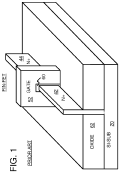
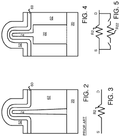
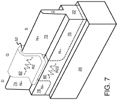
Step fin field-effect-transistor (FinFET) with slim top of fin and thick bottom of fin for electro-static-discharge (ESD) or electrical over-stress (EOS) protection
PatentActiveUS10510743B2
Innovation
- A hybrid FinFET design with a step fin structure, featuring a thicker bottom fin and a slim top fin, allows for enhanced ESD current handling by shunting excess current through the thicker bottom fin, reducing localized heating and maintaining optimal transistor characteristics for normal operation.
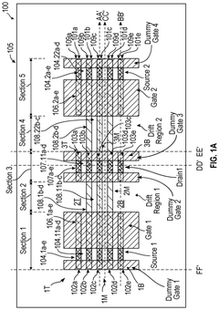
Fin-based field effect transistor (finFET) device with enhanced on-resistance and breakdown voltage
PatentActiveUS12113065B2
Innovation
- The implementation of a finFET device with a specific structure and fabrication flow that includes multiple alternating regions of n-type and p-type doped semiconductor, utilizing a super junction LDMOS structure, which allows for a lower Ron and higher breakdown voltage without additional mask or process steps, by optimizing the number and arrangement of fin portions in the drift regions.
Power-Performance-Area Tradeoffs
In the FinFET architecture, power, performance, and area (PPA) represent the critical triangle of trade-offs that designers must carefully balance. Signal integrity testing reveals that FinFET technology offers significant advantages in managing these trade-offs compared to planar transistors. The three-dimensional fin structure provides better electrostatic control of the channel, allowing for reduced leakage current while maintaining high drive current capability.
Power consumption analysis from signal integrity tests demonstrates that FinFETs typically achieve 30-40% lower dynamic power consumption at equivalent performance levels compared to planar technologies. This power efficiency stems from the ability to operate at lower supply voltages while maintaining performance targets. Static power reduction is even more pronounced, with up to 90% reduction in leakage current in some benchmark tests, particularly beneficial for battery-powered applications where standby power is critical.
Performance metrics from signal integrity testing show that FinFETs deliver 20-25% higher switching speeds at iso-power conditions. The improved channel control enables faster charging and discharging of load capacitances, resulting in reduced signal propagation delays. Signal integrity tests specifically highlight improved resistance to noise coupling between adjacent signal lines, with cross-talk reduction of approximately 15-20% compared to planar technologies at equivalent dimensions.
Area efficiency presents a more complex picture. While individual FinFET transistors can be smaller than their planar counterparts for equivalent drive strength, the three-dimensional structure introduces additional manufacturing complexity. Signal integrity tests reveal that the fin pitch and height must be carefully optimized to balance area efficiency with performance. Current generation FinFETs typically achieve 40-50% area reduction for the same functionality, though this advantage diminishes at advanced nodes due to more complex design rules.
The PPA trade-off optimization varies significantly based on application requirements. For high-performance computing applications, signal integrity tests indicate that optimizing for maximum performance while accepting higher power density is preferable. Conversely, mobile applications benefit from configurations that minimize power consumption while maintaining adequate performance thresholds. IoT applications typically prioritize area efficiency and ultra-low power consumption, even at the expense of peak performance capabilities.
Semiconductor Industry Standards Compliance
Semiconductor Industry Standards Compliance in FinFET signal integrity testing requires adherence to multiple international and industry-specific standards. The Joint Electron Device Engineering Council (JEDEC) provides the primary framework for signal integrity testing methodologies, particularly through standards like JESD22-B111 for package level signal integrity and JESD204C for high-speed serial interfaces. These standards establish critical parameters for signal integrity evaluation including jitter tolerance, eye diagram specifications, and impedance matching requirements.
The International Electrotechnical Commission (IEC) contributes complementary standards, notably IEC 62132 for electromagnetic compatibility testing and IEC 61967 for integrated circuit emissions measurement. For FinFET technology specifically, compliance with these standards ensures reliable performance across varying operating conditions and integration scenarios.
The Semiconductor Equipment and Materials International (SEMI) organization provides additional standards focusing on manufacturing process consistency that directly impacts signal integrity. SEMI F47 addresses voltage sag immunity while SEMI E176 covers test method standards for high-frequency measurements critical to FinFET signal characterization.
Testing methodologies must align with IEEE standards, particularly IEEE 1149.6 for advanced digital networks and IEEE 802.3 for Ethernet implementations where FinFET devices are increasingly deployed. The compliance verification process typically involves three-tier testing: component-level verification, system-level integration testing, and environmental stress testing under varied conditions.
Signal integrity compliance documentation requires comprehensive reporting of test conditions, equipment calibration records, and measurement uncertainties. The International Laboratory Accreditation Cooperation (ILAC) guidelines establish the framework for test result validation and cross-laboratory consistency, ensuring global acceptance of compliance certifications.
Recent developments in standards compliance include the introduction of statistical analysis requirements for process variation impacts on signal integrity. The Statistical Analysis of Random Telegraph Noise (RTN) has become mandatory for advanced FinFET nodes below 7nm, as specified in updated JEDEC standards. This addresses the increasing concern about transient noise effects on signal reliability in highly scaled devices.
Compliance challenges specific to FinFET technology include quantifying the impact of self-heating effects on signal integrity and establishing appropriate de-rating factors for high-frequency operation. Industry consortia like the Silicon Integration Initiative (Si2) are currently developing supplementary guidelines to address these FinFET-specific concerns, expected to be formalized in upcoming standard revisions.
Unlock deeper insights with PatSnap Eureka Quick Research — get a full tech report to explore trends and direct your research. Try now!
Generate Your Research Report Instantly with AI Agent
Supercharge your innovation with PatSnap Eureka AI Agent Platform!
