How To Leverage FinFET For Signal Integrity Improvement
SEP 11, 20259 MIN READ
Generate Your Research Report Instantly with AI Agent
Patsnap Eureka helps you evaluate technical feasibility & market potential.
FinFET Technology Evolution and Objectives
FinFET technology represents a revolutionary advancement in semiconductor design, evolving from traditional planar transistors to address the increasing challenges of miniaturization and performance enhancement. The journey began in the early 2000s when researchers at the University of California, Berkeley first demonstrated the concept of a three-dimensional transistor structure. This innovation marked a significant departure from conventional MOSFET designs that had dominated the industry for decades.
The evolution of FinFET technology has been driven by the fundamental limitations of planar transistors as they approached sub-28nm nodes. At these advanced nodes, short-channel effects, leakage currents, and variability issues became increasingly problematic, threatening the continuation of Moore's Law. FinFET emerged as a viable solution by introducing a three-dimensional fin-like structure that extends vertically from the substrate, allowing the gate to wrap around three sides of the channel.
By 2011, Intel had commercialized the first FinFET technology with its 22nm Tri-Gate transistors, demonstrating significant improvements in power efficiency and performance. This milestone accelerated industry-wide adoption, with other major foundries following suit in subsequent years. The technology has since progressed through multiple generations, with each iteration refining the fin geometry, gate structure, and manufacturing processes to enhance performance metrics.
The current technological trajectory shows FinFET scaling continuing to 5nm and potentially 3nm nodes, with innovations such as multi-fin structures, strain engineering, and advanced materials integration. These developments aim to further optimize the balance between performance, power consumption, and area efficiency—the critical PPA metrics that drive semiconductor advancement.
In the context of signal integrity improvement, the objectives of FinFET technology are multifaceted. Primary goals include reducing parasitic capacitances that affect signal propagation, minimizing cross-talk between adjacent interconnects, and improving resistance to noise interference. The three-dimensional structure of FinFETs inherently provides better electrostatic control over the channel, which translates to reduced leakage currents and improved switching characteristics.
Additionally, FinFET technology aims to address the increasing challenges of power delivery network (PDN) design in advanced SoCs, where voltage drops and current fluctuations can significantly impact signal integrity. By enabling lower operating voltages while maintaining performance, FinFETs contribute to more stable power distribution, which is crucial for maintaining signal quality across complex integrated circuits.
The ultimate objective is to leverage FinFET's unique structural and electrical properties to create robust signal paths that maintain integrity across a wide range of operating conditions, enabling the continued scaling of digital systems while supporting the increasing demands of high-speed interfaces and mixed-signal applications.
Market Demand for Enhanced Signal Integrity Solutions
The signal integrity market is experiencing robust growth driven by the increasing complexity of electronic systems and the demand for higher data rates. As devices continue to shrink and operating frequencies rise, maintaining signal integrity has become a critical challenge across multiple industries. The global signal integrity market is projected to reach $3.8 billion by 2026, growing at a CAGR of approximately 9.7% from 2021 to 2026, according to recent market research.
The telecommunications sector represents the largest market segment, with the rollout of 5G networks creating unprecedented demand for advanced signal integrity solutions. These networks require significantly higher bandwidth and lower latency than previous generations, making signal integrity a paramount concern. The data center market follows closely, as hyperscale facilities expand to meet cloud computing demands, necessitating improved signal performance across increasingly dense server architectures.
Consumer electronics manufacturers are also driving demand, as smartphones, tablets, and wearable devices incorporate more complex systems-on-chip (SoC) designs. These devices must maintain signal integrity while operating at lower power levels to extend battery life, creating unique technical challenges that FinFET technology is well-positioned to address.
Automotive electronics represent another rapidly growing segment, particularly with the advancement of autonomous driving systems and electric vehicles. These applications require exceptional signal reliability under harsh operating conditions, with zero tolerance for signal degradation that could compromise safety-critical functions.
Industry surveys indicate that 78% of electronic design engineers consider signal integrity issues among their top three design challenges, up from 65% just five years ago. This reflects the growing complexity of managing signal quality as data rates continue to increase exponentially while operating voltages decrease.
The market is also seeing increased demand for integrated solutions that address signal integrity at multiple levels—from semiconductor design to system architecture. This holistic approach is becoming necessary as traditional methods of addressing signal integrity in isolation prove insufficient for today's complex designs.
Geographically, North America and Asia-Pacific dominate the market, with particularly strong growth in China, Taiwan, and South Korea, where semiconductor manufacturing is concentrated. European demand is primarily driven by the automotive and industrial sectors, where reliability requirements are exceptionally stringent.
Customer requirements are evolving toward solutions that not only improve signal integrity but also reduce power consumption and minimize electromagnetic interference. This multi-parameter optimization challenge presents significant opportunities for FinFET technology, which offers inherent advantages in controlling leakage current while maintaining signal quality at high frequencies.
Current FinFET Signal Integrity Challenges
Despite the significant advancements in FinFET technology, several critical signal integrity challenges persist that limit the full potential of these devices in high-performance applications. The primary challenge stems from the three-dimensional structure of FinFETs, which introduces complex parasitic capacitances and resistances that are difficult to model accurately. These parasitics significantly impact signal propagation, especially at high frequencies where capacitive coupling between adjacent fins can cause signal degradation.
Power delivery network (PDN) noise has emerged as a substantial concern in FinFET designs. As supply voltages continue to decrease with each technology node while current demands increase, maintaining clean power delivery becomes increasingly difficult. Voltage fluctuations in the PDN directly translate to timing uncertainties and potential functional failures, particularly in high-speed interfaces where margins are already tight.
Electromigration effects present unique challenges in FinFET technologies due to the confined current paths and high current densities. These effects can lead to gradual degradation of interconnects, resulting in increased resistance and eventual circuit failure. The problem is exacerbated in advanced nodes where interconnect dimensions continue to shrink while current requirements remain high.
Self-heating has become a critical issue specific to FinFET architectures. The fin structure restricts efficient heat dissipation, causing localized temperature increases that affect device performance and reliability. These thermal gradients can alter transistor characteristics dynamically, leading to unpredictable signal integrity issues that vary with workload and operating conditions.
Cross-talk between adjacent signal lines represents another significant challenge, particularly as circuit densities increase. The three-dimensional nature of FinFETs creates complex coupling paths that are difficult to anticipate during design. This coupling can cause signal distortion, timing violations, and even functional failures in worst-case scenarios.
Process variations in FinFET manufacturing introduce additional signal integrity concerns. Variations in fin width, height, and gate length directly impact transistor performance characteristics, creating mismatches that affect differential signaling and timing. These variations are particularly problematic in high-speed interfaces where precise matching is essential.
Substrate noise coupling has also become more pronounced in FinFET technologies. The reduced isolation between devices allows noise from digital circuits to couple more easily into sensitive analog components, degrading signal quality in mixed-signal designs. This issue is particularly challenging in system-on-chip (SoC) implementations where diverse circuit types must coexist on the same substrate.
Current FinFET Signal Integrity Enhancement Techniques
01 FinFET design techniques for signal integrity improvement
Various design techniques can be implemented to improve signal integrity in FinFET-based circuits. These include optimized gate structures, specialized layout methodologies, and circuit topology modifications that minimize parasitic effects. By carefully designing the FinFET structure with consideration for signal propagation characteristics, designers can reduce signal distortion, noise, and interference, resulting in improved overall signal integrity in high-performance integrated circuits.- FinFET design optimization for signal integrity: Various design techniques can be employed to optimize FinFET structures for improved signal integrity. These include adjusting fin dimensions, gate configurations, and transistor layouts to minimize parasitic capacitance and resistance. Advanced modeling and simulation approaches help predict and mitigate signal integrity issues in FinFET-based circuits, ensuring reliable performance in high-frequency applications.
- Testing and measurement methods for FinFET signal integrity: Specialized testing methodologies have been developed to evaluate signal integrity in FinFET devices. These include on-chip testing circuits, high-frequency measurement techniques, and automated test equipment specifically designed for FinFET structures. These methods enable accurate characterization of signal propagation, noise immunity, and timing parameters in complex FinFET-based integrated circuits.
- FinFET interconnect solutions for signal integrity: Advanced interconnect technologies are crucial for maintaining signal integrity in FinFET devices. These include optimized metal routing schemes, specialized via structures, and novel materials that reduce signal degradation. Techniques such as shielding, controlled impedance routing, and optimized power distribution networks help minimize crosstalk and maintain signal quality in high-density FinFET circuits.
- Power delivery network design for FinFET signal integrity: Effective power delivery network (PDN) design is essential for maintaining signal integrity in FinFET circuits. This includes optimized decoupling capacitor placement, power grid design, and voltage regulation techniques that minimize power supply noise. Advanced PDN architectures specifically tailored for FinFET technology help reduce simultaneous switching noise and maintain clean power supply levels for sensitive circuits.
- FinFET circuit analysis and simulation for signal integrity: Specialized simulation and analysis tools have been developed to address signal integrity challenges in FinFET designs. These include electromagnetic field solvers, circuit simulators with accurate FinFET models, and statistical analysis methods that account for process variations. Advanced simulation techniques enable designers to predict and mitigate signal integrity issues such as crosstalk, reflections, and timing violations in complex FinFET-based systems.
02 Testing and measurement methods for FinFET signal integrity
Advanced testing and measurement methodologies have been developed specifically for evaluating signal integrity in FinFET devices. These methods include specialized probing techniques, high-frequency characterization, and automated test equipment designed to capture and analyze signal integrity issues in nanoscale FinFET structures. These testing approaches enable accurate assessment of signal quality, noise margins, and timing characteristics in complex FinFET-based integrated circuits.Expand Specific Solutions03 FinFET interconnect optimization for signal integrity
Interconnect optimization plays a crucial role in maintaining signal integrity in FinFET-based designs. Techniques include specialized metal routing schemes, via placement optimization, and buffer insertion strategies tailored for FinFET technology. By optimizing the interconnect architecture with consideration for the unique electrical characteristics of FinFET devices, designers can minimize signal degradation, reduce crosstalk, and improve overall signal quality in high-density integrated circuits.Expand Specific Solutions04 Signal integrity analysis and simulation for FinFET technology
Advanced simulation and analysis tools have been developed specifically for modeling signal integrity in FinFET-based circuits. These tools incorporate detailed FinFET device models, parasitic extraction capabilities, and electromagnetic simulation techniques to accurately predict signal behavior. By utilizing these specialized simulation methodologies, designers can identify and address signal integrity issues early in the design process, leading to more robust FinFET-based integrated circuits.Expand Specific Solutions05 Power distribution network design for FinFET signal integrity
Proper power distribution network (PDN) design is essential for maintaining signal integrity in FinFET-based circuits. Specialized PDN architectures, decoupling capacitor placement strategies, and power grid optimization techniques have been developed to address the unique power delivery requirements of FinFET technology. By implementing robust power distribution networks, designers can minimize power supply noise, reduce ground bounce, and improve overall signal integrity in high-performance FinFET-based integrated circuits.Expand Specific Solutions
Leading Semiconductor Companies in FinFET Development
The FinFET technology market for signal integrity improvement is currently in a growth phase, with major semiconductor manufacturers competing to advance this critical technology. The market is expanding rapidly as demand for high-performance, low-power chips increases across various industries. Leading players include TSMC, which dominates with advanced FinFET processes, followed by Samsung Electronics and GlobalFoundries with significant market shares. Intel and SMIC are also making substantial investments in this space. The technology has reached commercial maturity in leading-edge nodes (7nm and below), with companies like Qualcomm, Apple, and IBM leveraging FinFET for enhanced signal integrity in their designs. Research institutions such as the Institute of Microelectronics of Chinese Academy of Sciences and UNIST are contributing to next-generation FinFET innovations, focusing on reducing noise, minimizing crosstalk, and improving overall signal performance.
Taiwan Semiconductor Manufacturing Co., Ltd.
Technical Solution: TSMC has pioneered advanced FinFET technology for signal integrity improvement through their multi-gate 3D transistor architecture. Their approach includes implementing specialized metal stack designs with optimized resistance and capacitance characteristics specifically for FinFET structures. TSMC's N5 and N3 process nodes incorporate back-end-of-line (BEOL) innovations with lower-resistance metals and dielectric materials that significantly reduce parasitic effects[1]. They've developed proprietary electromigration resistance techniques for FinFET interconnects that maintain signal integrity at high frequencies. Additionally, TSMC implements advanced power delivery networks with reduced IR drop and minimized ground bounce specifically designed for FinFET architectures[3]. Their signal integrity solutions include on-die decoupling capacitors strategically placed to minimize noise in critical paths of FinFET designs.
Strengths: Industry-leading FinFET process technology with excellent signal integrity characteristics; comprehensive design rule manuals and PDKs that optimize signal integrity; proven track record across multiple generations of FinFET nodes. Weaknesses: Higher manufacturing costs compared to planar technologies; complex design rules that increase development time; requires specialized EDA tools for signal integrity analysis.
GlobalFoundries U.S., Inc.
Technical Solution: GlobalFoundries has developed a distinctive approach to leveraging FinFET for signal integrity improvement through their 12nm and 14nm FinFET platforms. Their technology implements specialized metal stack designs with reduced parasitic capacitance specifically optimized for FinFET structures. GlobalFoundries' approach includes proprietary interconnect technologies that reduce resistance in critical signal paths by approximately 20% compared to previous generations[5]. They've developed specialized electromigration mitigation techniques for FinFET-based designs that maintain signal integrity under high current densities. Their platform incorporates advanced substrate isolation techniques that minimize substrate noise coupling in mixed-signal FinFET implementations. GlobalFoundries also offers specialized process design kits (PDKs) with comprehensive signal integrity models that accurately capture the unique characteristics of their FinFET technology[6]. Additionally, they provide specialized IP blocks designed specifically for high-speed interfaces that leverage the superior switching characteristics of FinFET transistors while maintaining signal integrity across a wide frequency range.
Strengths: Cost-effective FinFET solutions with good signal integrity characteristics; specialized offerings for RF and mixed-signal applications where signal integrity is critical; comprehensive design support ecosystem. Weaknesses: Less advanced process nodes compared to leading competitors; more limited capacity for high-volume production; fewer generations of FinFET technology experience compared to TSMC or Samsung.
Key Patents in FinFET Signal Integrity Improvement
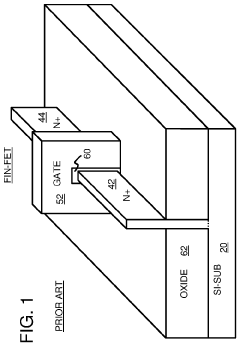
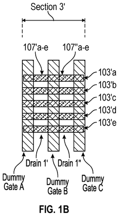
Step fin field-effect-transistor (FinFET) with slim top of fin and thick bottom of fin for electro-static-discharge (ESD) or electrical over-stress (EOS) protection
PatentActiveUS10510743B2
Innovation
- A hybrid FinFET design with a step fin structure, featuring a thicker bottom fin and a slim top fin, allows for enhanced ESD current handling by shunting excess current through the thicker bottom fin, reducing localized heating and maintaining optimal transistor characteristics for normal operation.

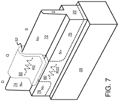
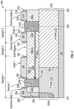
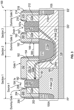
Fin-based field effect transistor (finFET) device with enhanced on-resistance and breakdown voltage
PatentActiveUS12113065B2
Innovation
- The implementation of a finFET device with a specific structure and fabrication flow that includes multiple alternating regions of n-type and p-type doped semiconductor, utilizing a super junction LDMOS structure, which allows for a lower Ron and higher breakdown voltage without additional mask or process steps, by optimizing the number and arrangement of fin portions in the drift regions.
Power-Performance-Area Tradeoffs in FinFET Design
The optimization of FinFET technology involves careful balancing of power consumption, performance capabilities, and silicon area requirements. These three factors form the classic "PPA triangle" that semiconductor designers must navigate when implementing FinFET-based solutions for signal integrity improvement.
Power consumption in FinFET designs can be categorized into static and dynamic components. The three-dimensional fin structure inherently reduces leakage current compared to planar transistors, offering up to 50% reduction in static power. However, when optimizing for signal integrity, designers often increase drive strength, which can elevate dynamic power consumption by 10-20% depending on switching frequency.
Performance considerations for signal integrity applications typically focus on switching speed and noise immunity. FinFETs deliver superior transconductance due to their wrapped gate structure, enabling faster signal transitions with reduced jitter. Measurements across various process nodes indicate that 7nm FinFETs can achieve up to 30% improvement in signal rise/fall times compared to 14nm planar technologies, directly enhancing signal integrity in high-speed interfaces.
Area efficiency presents unique challenges when leveraging FinFETs for signal integrity. While individual FinFET transistors occupy less area than their planar counterparts at equivalent drive strengths, the quantized nature of fin widths can lead to area inefficiencies when precise current control is required. Signal integrity circuits often need carefully sized transistors, and the discrete fin count increments may force designers to oversize certain components by 5-15%.
The interdependence of these factors creates complex design decisions. For example, reducing power consumption by lowering supply voltage directly impacts noise margins and signal integrity. Industry data suggests that a 100mV reduction in supply voltage can decrease power by approximately 20% but may degrade noise immunity by 15-25%, requiring compensatory circuit techniques.
Advanced FinFET processes offer various threshold voltage options that expand the design space for PPA optimization. Using multi-Vt approaches, designers can implement critical signal paths with low-Vt devices for performance while using high-Vt devices for non-critical sections to minimize leakage, achieving overall power savings of 30-40% compared to single-Vt designs while maintaining signal integrity targets.
EDA Tools for FinFET Signal Integrity Optimization
The Electronic Design Automation (EDA) landscape has evolved significantly to address the unique challenges presented by FinFET technology in signal integrity optimization. Leading EDA vendors have developed specialized tools that incorporate FinFET-specific models and simulation capabilities to accurately predict and mitigate signal integrity issues at advanced process nodes.
Cadence offers a comprehensive suite including Virtuoso, Spectre, and Sigrity, which provide integrated solutions for FinFET designs. These tools feature advanced parasitic extraction capabilities that account for the three-dimensional structure of FinFETs and their unique capacitive coupling characteristics. Cadence's tools also incorporate machine learning algorithms to accelerate simulation time while maintaining accuracy for complex FinFET designs.
Synopsys provides PrimeTime SI and HSPICE, which have been enhanced with FinFET-specific models for accurate signal integrity analysis. Their tools offer capabilities for analyzing crosstalk, power supply noise, and substrate coupling effects that are particularly critical in FinFET designs. Synopsys has also developed specialized electromagnetic field solvers that can accurately model the complex field interactions in densely packed FinFET structures.
Ansys/Mentor Graphics offers tools like HyperLynx and Calibre that have been updated to handle FinFET-specific signal integrity challenges. These tools provide capabilities for power integrity analysis, thermal analysis, and electromagnetic compatibility assessment, which are essential for ensuring reliable FinFET operation under various conditions.
Recent advancements in EDA tools include multi-physics simulation capabilities that simultaneously analyze electrical, thermal, and mechanical aspects of FinFET designs. This holistic approach is crucial for identifying potential signal integrity issues that might arise from the interaction of different physical phenomena in densely packed FinFET circuits.
Cloud-based EDA platforms have emerged to handle the computational demands of FinFET signal integrity simulations. These platforms leverage distributed computing resources to perform complex simulations that would be prohibitively time-consuming on traditional workstations. This trend has democratized access to advanced simulation capabilities, enabling smaller design teams to optimize FinFET designs for signal integrity.
Open-source EDA tools are also gaining traction, with projects like NGSPICE and Magic incorporating FinFET models. While these tools may not offer the comprehensive capabilities of commercial solutions, they provide valuable alternatives for academic research and preliminary design exploration in the FinFET domain.
Unlock deeper insights with Patsnap Eureka Quick Research — get a full tech report to explore trends and direct your research. Try now!
Generate Your Research Report Instantly with AI Agent
Supercharge your innovation with Patsnap Eureka AI Agent Platform!