FinFET Vs SOI: Which Offers Better Density?
SEP 11, 20259 MIN READ
Generate Your Research Report Instantly with AI Agent
Patsnap Eureka helps you evaluate technical feasibility & market potential.
FinFET and SOI Technology Evolution and Objectives
The semiconductor industry has witnessed a remarkable evolution in transistor architecture over the past decades, transitioning from planar MOSFETs to more advanced three-dimensional structures. FinFET and Silicon-on-Insulator (SOI) technologies represent two significant milestones in this journey, each developed to address the scaling limitations of conventional transistors as device dimensions approached the nanometer scale.
FinFET technology emerged in the early 2000s as a revolutionary approach to combat short-channel effects that plagued planar transistors. By creating a fin-like structure that extends vertically from the substrate, FinFETs enabled better electrostatic control of the channel, significantly reducing leakage current. Intel's introduction of Tri-Gate transistors (their version of FinFET) at the 22nm node in 2011 marked the commercial viability of this technology, setting a new industry standard.
Concurrently, SOI technology evolved along a different path. By introducing an insulating layer between the active device layer and the substrate, SOI offered improved electrical isolation, reduced parasitic capacitances, and enhanced performance characteristics. SOI has diversified into several variants, including Partially Depleted SOI (PDSOI), Fully Depleted SOI (FDSOI), and more recently, Ultra-Thin Body and BOX (UTBB) SOI, each addressing specific technical challenges.
The technological objectives driving both FinFET and SOI development share common ground: achieving higher transistor density, improving performance, reducing power consumption, and maintaining manufacturing feasibility at advanced nodes. However, their approaches to these objectives differ fundamentally. FinFET technology prioritizes three-dimensional channel control to maximize current drive in a minimal footprint, while SOI focuses on optimizing the substrate architecture to enhance electrical characteristics.
The density question between these technologies has become increasingly critical as the industry pushes toward the 5nm node and beyond. FinFETs have demonstrated exceptional scaling capabilities, with leading manufacturers implementing multi-fin designs and continuously reducing fin pitch. Meanwhile, FDSOI has positioned itself as a compelling alternative, particularly for applications where power efficiency is paramount.
Recent technological trends indicate a convergence of these approaches, with hybrid solutions emerging that combine aspects of both technologies. For instance, FinFETs built on SOI substrates represent an attempt to harness the advantages of both architectures. Additionally, the industry is exploring gate-all-around (GAA) transistors and nanowire/nanosheet designs as potential successors to both FinFET and SOI for sub-3nm nodes.
The evolution trajectory suggests that neither technology represents an endpoint, but rather transitional stages in the semiconductor roadmap. As quantum effects become increasingly dominant at smaller nodes, fundamental rethinking of transistor design continues to drive innovation in this space.
Market Demand Analysis for Advanced Semiconductor Nodes
The semiconductor industry's demand for advanced nodes continues to accelerate, driven primarily by applications requiring higher performance, lower power consumption, and increased transistor density. Market analysis indicates that the global semiconductor foundry market is experiencing robust growth, with advanced nodes (10nm and below) representing the fastest-growing segment. This growth is fueled by expanding applications in artificial intelligence, high-performance computing, 5G infrastructure, and autonomous vehicles.
When examining market demand specifically related to FinFET versus SOI technologies, several distinct trends emerge. FinFET technology has gained significant market traction in high-performance applications due to its superior scaling capabilities and performance characteristics at advanced nodes. Major foundries including TSMC, Samsung, and Intel have heavily invested in FinFET processes for their leading-edge offerings, responding to demand from premium smartphone processors, data center chips, and AI accelerators.
Meanwhile, SOI technology, particularly Fully Depleted SOI (FD-SOI), has carved out a growing market niche in IoT, automotive, and RF applications where power efficiency and cost considerations often outweigh absolute density requirements. GlobalFoundries and Samsung have developed dedicated FD-SOI process nodes to address this segment of the market.
Market forecasts suggest that by 2025, chips manufactured at advanced nodes will account for approximately 40% of total semiconductor revenue, despite representing less than 10% of total silicon area produced. This economic reality underscores the premium value placed on advanced node capabilities, where the density advantage of FinFET becomes particularly significant.
Customer demand patterns reveal an interesting bifurcation in the market. High-volume manufacturers of premium mobile SoCs, GPUs, and server processors consistently prioritize the density advantages of FinFET technology, accepting the associated higher manufacturing costs. Conversely, manufacturers of edge computing devices, automotive microcontrollers, and analog/RF components often favor the balanced approach of SOI technology, which offers sufficient performance with better power characteristics and potentially lower costs at certain nodes.
Regional market analysis shows that East Asia continues to dominate demand for advanced node manufacturing, with North America representing the largest market for design of chips utilizing these technologies. Europe has shown particular interest in FD-SOI technology, partly due to strong regional expertise in automotive and industrial applications where this technology excels.
The market is also witnessing increased interest in hybrid approaches that combine aspects of both technologies, indicating that future demand may evolve toward specialized process technologies optimized for specific application domains rather than a one-size-fits-all approach to semiconductor manufacturing.
Current Challenges in Transistor Scaling Technologies
The semiconductor industry's relentless pursuit of Moore's Law has encountered significant obstacles as transistor dimensions approach atomic scales. Traditional planar transistor architectures have reached their physical limits, necessitating the development of advanced 3D structures like FinFET and Silicon-on-Insulator (SOI) technologies. These innovations represent different approaches to addressing the fundamental challenges of transistor scaling.
Short-channel effects (SCEs) constitute one of the most critical challenges in modern transistor design. As gate lengths shrink below 20nm, quantum tunneling and gate leakage increase exponentially, degrading device performance and increasing power consumption. Both FinFET and SOI technologies attempt to mitigate these effects through improved electrostatic control, but employ fundamentally different architectural approaches.
Power density management presents another significant hurdle. With billions of transistors packed onto modern chips, heat dissipation has become a limiting factor in performance scaling. The semiconductor industry faces a thermal wall that constrains clock speeds and operational voltages. This challenge is particularly relevant when comparing FinFET and SOI technologies, as their thermal characteristics and power profiles differ substantially.
Process variability increases dramatically at advanced nodes, affecting transistor performance consistency across chips. As dimensions shrink, atomic-level variations in dopant distribution, gate oxide thickness, and channel dimensions have proportionally larger impacts on device characteristics. Manufacturing yield and reliability become increasingly difficult to maintain, requiring sophisticated compensation techniques.
Integration complexity represents a formidable challenge for both technologies. FinFET structures demand precise fin formation with consistent height and width, while SOI requires specialized wafer manufacturing processes. The cost implications of these complex fabrication requirements cannot be overlooked, as they directly impact the economic viability of continued scaling.
Parasitic capacitance effects become increasingly dominant at smaller nodes, limiting switching speed and power efficiency. The three-dimensional nature of FinFETs introduces additional parasitic elements compared to planar designs, while SOI's insulating layer helps reduce certain parasitic components but introduces others through body effects.
Material limitations are pushing researchers toward novel solutions. Silicon's intrinsic properties are being stretched to their theoretical limits, prompting exploration of alternative channel materials like germanium, III-V compounds, and two-dimensional materials. Both FinFET and SOI platforms must accommodate these material innovations to extend scaling benefits.
The density comparison between FinFET and SOI technologies must be evaluated within this complex landscape of challenges. Each technology offers distinct advantages and compromises in addressing these fundamental scaling limitations, with implications extending beyond simple area metrics to encompass performance, power efficiency, and manufacturability considerations.
Comparative Analysis of FinFET vs SOI Density Solutions
01 Integration of FinFET with SOI for improved device density
The combination of FinFET architecture with Silicon-On-Insulator (SOI) substrates enables significant improvements in device density. This integration leverages the three-dimensional structure of FinFETs with the superior insulation properties of SOI, resulting in reduced leakage currents and better electrostatic control. The buried oxide layer in SOI substrates helps to minimize parasitic capacitances, allowing for closer device placement and higher integration density in advanced semiconductor nodes.- Integration of FinFET with SOI for improved device density: The combination of FinFET architecture with Silicon-On-Insulator (SOI) substrate technology enables significant improvements in device density. This integration leverages the three-dimensional structure of FinFETs with the superior insulation properties of SOI to create more compact transistors. The buried oxide layer in SOI reduces parasitic capacitance and leakage currents, allowing for tighter packing of FinFET devices without performance degradation, ultimately leading to higher integration density in semiconductor chips.
- Advanced manufacturing techniques for high-density FinFET-SOI structures: Specialized manufacturing techniques have been developed to achieve higher density in FinFET-SOI devices. These include optimized fin formation processes, self-aligned double patterning, and selective epitaxial growth methods. Advanced lithography and etching techniques enable the creation of narrower fins with precise dimensions and spacing. Additionally, novel gate formation processes and contact schemes have been implemented to reduce the overall footprint of FinFET devices on SOI substrates, contributing to increased transistor density while maintaining electrical performance.
- Multi-fin and multi-gate architectures for enhanced density: Multi-fin and multi-gate architectures in FinFET-SOI technology significantly increase transistor density. By implementing multiple fins per transistor and utilizing gate structures that wrap around multiple sides of each fin, these designs maximize the effective channel width while minimizing the lateral footprint. This approach allows for higher current drive capability within a smaller area. Various configurations such as dual-gate, tri-gate, and gate-all-around structures have been developed to optimize the trade-off between performance and density in SOI-based FinFET devices.
- Ultra-thin body SOI for FinFET density scaling: Ultra-thin body SOI substrates enable significant density improvements in FinFET technology. By reducing the silicon layer thickness to nanometer scale, these substrates allow for better electrostatic control of the channel and reduced short-channel effects. This enables further scaling of gate length and fin width without performance degradation. The combination of ultra-thin SOI with FinFET structures facilitates the creation of fully depleted devices with superior electrical characteristics at smaller dimensions, supporting continued density scaling beyond conventional bulk silicon approaches.
- 3D integration and stacking techniques for FinFET-SOI devices: Three-dimensional integration and stacking techniques applied to FinFET-SOI technology enable dramatic increases in device density. By vertically stacking multiple layers of FinFET devices on SOI substrates, these approaches multiply the effective transistor density per unit area. Advanced through-silicon via (TSV) technology, layer transfer methods, and monolithic 3D integration techniques facilitate the electrical connections between stacked device layers. The inherent isolation properties of SOI substrates are particularly advantageous in these 3D architectures, reducing crosstalk between vertically adjacent devices and enabling higher integration density.
02 Multi-fin structures for enhanced transistor density
Multi-fin structures in FinFET technology provide a method to increase current drive capability while maintaining a small footprint. By implementing multiple fins within a single transistor, the effective channel width is increased without expanding the lateral dimensions of the device. This approach allows for higher transistor density in SOI-based FinFET designs, as the vertical nature of the fins utilizes the third dimension for scaling rather than consuming additional horizontal space on the silicon substrate.Expand Specific Solutions03 Novel SOI substrate modifications for FinFET density optimization
Specialized modifications to SOI substrates can enhance the integration density of FinFET devices. These modifications include varying the thickness of the silicon and buried oxide layers, implementing localized SOI regions, or creating hybrid substrates. Such customized SOI platforms provide optimal conditions for high-density FinFET fabrication by allowing precise control over fin formation, isolation between devices, and management of thermal characteristics, all of which contribute to achieving higher device densities.Expand Specific Solutions04 Advanced isolation techniques for high-density FinFET-SOI integration
Innovative isolation methods are crucial for maximizing device density in FinFET-SOI technologies. These techniques include shallow trench isolation (STI), enhanced dielectric isolation layers, and novel fin separation approaches. By effectively isolating individual fins and transistors while minimizing the isolation area requirements, these methods enable closer device placement. The inherent isolation properties of SOI substrates, when combined with these advanced techniques, allow for significant reductions in the minimum spacing between active devices.Expand Specific Solutions05 3D integration strategies for FinFET-SOI density scaling
Three-dimensional integration strategies represent a frontier approach to increasing device density in FinFET-SOI technologies. These include vertical stacking of transistors, implementation of monolithic 3D integration, and development of novel interconnect schemes specifically designed for 3D architectures. By utilizing the vertical dimension more effectively, these approaches enable dramatic increases in functional density beyond what is possible with traditional planar scaling. The combination of SOI's excellent layer transfer capabilities with FinFET's inherent 3D structure makes this technology pairing particularly suitable for advanced 3D integration.Expand Specific Solutions
Key Semiconductor Manufacturers and IP Providers
The FinFET vs SOI density competition represents a critical battleground in semiconductor technology, currently in a mature development phase with established market applications. Major players like TSMC and IBM have taken different strategic positions, with TSMC championing FinFET technology for high-performance computing applications while IBM has invested heavily in SOI technology, particularly for power-efficient applications. GlobalFoundries offers both technologies, positioning itself as a versatile supplier. The market shows a bifurcation trend where FinFET dominates high-density applications while SOI finds advantages in specific power-sensitive segments. Recent advancements from research institutions like IMEC and semiconductor manufacturers including Samsung and UMC continue to push both technologies toward their theoretical density limits.
International Business Machines Corp.
Technical Solution: IBM has pioneered advanced SOI technology while also developing FinFET solutions, giving them unique perspective on both approaches. Their SOI implementation focuses on Partially Depleted SOI (PD-SOI) and Fully Depleted SOI (FD-SOI) variants. IBM's research demonstrates that while FinFETs generally offer better density scaling at leading-edge nodes (7nm and below), their enhanced SOI technology provides competitive density at 14nm-22nm nodes with additional benefits[5]. IBM's Power processors utilizing SOI technology achieve high performance while maintaining reasonable transistor densities. Their research shows that SOI can achieve approximately 85-90% of the density of equivalent FinFET nodes at 14nm, but this gap widens at smaller geometries. IBM has also explored hybrid approaches that combine aspects of both technologies to optimize for specific applications. Their work with extremely thin SOI (ETSOI) demonstrated potential density improvements while maintaining the fundamental SOI advantages of reduced parasitic capacitance and improved isolation[6].
Strengths: Better RF performance and analog characteristics; reduced parasitic capacitance; simplified process integration for certain applications; superior soft-error immunity; better thermal isolation. Weaknesses: Density disadvantage becomes more pronounced at nodes below 14nm; higher substrate costs; floating body effects in some implementations; more complex design considerations for some circuit types.
GLOBALFOUNDRIES, Inc.
Technical Solution: GlobalFoundries has strategically focused on Fully Depleted Silicon-On-Insulator (FD-SOI) technology with their 22FDX and 12FDX platforms. Their FD-SOI approach utilizes an ultra-thin layer of silicon over a buried oxide insulator, which provides full depletion of the transistor channel without requiring the 3D fin structure of FinFETs. GlobalFoundries' 22FDX platform achieves transistor densities comparable to 14/16nm FinFET technologies but with significantly reduced manufacturing complexity[3]. The 12FDX platform further improves density while maintaining the SOI advantages. Their SOI implementation enables body biasing techniques that allow dynamic performance/power optimization, which is particularly valuable for IoT and RF applications. The planar nature of FD-SOI allows for simpler manufacturing processes with fewer masks and processing steps compared to FinFET, resulting in lower production costs while still achieving competitive densities for many applications[4].
Strengths: Simpler manufacturing process with fewer masks; excellent electrostatics without 3D structures; superior RF performance; effective body biasing capabilities for power management; lower production costs. Weaknesses: Limited scaling potential beyond 12nm compared to FinFET; slightly lower maximum performance at the same node; smaller ecosystem of design tools and IP compared to mainstream FinFET.
Critical Patents and Research in Transistor Density Enhancement
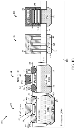
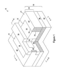
Nanosheet (NS) and fin field-effect transistor (FinFET) hybrid integration
PatentActiveUS11545483B2
Innovation
- A semiconductor device integrating silicon-on-insulator (SOI) transistors, fin field-effect transistors (FinFETs), and gate-all-around (GAA) transistors is fabricated, utilizing a substrate with specific crystal orientations and structures like backside deep n-wells, nanosheets, and shallow trench isolation to enhance electrostatic control and mobility.

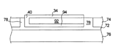
Silicon on insulator field effect transistor with heterojunction gate
PatentInactiveUS6759308B2
Innovation
- A silicon on insulator field effect transistor structure with a heterojunction gate and backgate formed from silicon carbide, doped with impurities to control carrier types and densities, reducing junction capacitance and improving channel control.
Power-Performance-Area (PPA) Trade-offs Analysis
The Power-Performance-Area (PPA) trade-off analysis between FinFET and SOI technologies reveals critical considerations for semiconductor manufacturers and designers. FinFET technology generally offers superior performance characteristics at high frequencies, with reduced leakage current compared to planar transistors. This translates to approximately 25-30% performance improvement at the same power envelope when compared to conventional planar technologies.
SOI technology, particularly Fully Depleted SOI (FD-SOI), demonstrates excellent power efficiency advantages, especially at lower operating voltages. FD-SOI can operate at voltages as low as 0.6V while maintaining reasonable performance, offering up to 50% power reduction compared to bulk CMOS at equivalent performance points. This makes SOI particularly attractive for low-power and IoT applications where battery life is paramount.
When examining area considerations, FinFET typically provides better transistor density due to its three-dimensional structure. Current generation FinFET processes can achieve up to 15-20% higher transistor density compared to equivalent node SOI implementations. However, this density advantage comes with increased manufacturing complexity and higher mask counts, which directly impacts production costs.
The performance-power curve comparison shows that FinFET maintains performance advantages at higher voltages and frequencies, while SOI demonstrates better efficiency at the lower end of the voltage spectrum. The crossover point typically occurs around 0.8-0.9V, where the technologies show comparable efficiency metrics.
Manufacturing considerations also impact the PPA equation significantly. FinFET processes require more complex multi-patterning techniques and have stricter design rules, increasing both design and manufacturing costs. SOI, while requiring specialized wafer substrates, often features simpler process flows with fewer masks, potentially offsetting the initial wafer cost premium.
Thermal characteristics further differentiate these technologies, with SOI's buried oxide layer creating thermal insulation challenges that can impact sustained performance under heavy loads. FinFET's better thermal conductivity allows for more consistent performance under varying thermal conditions, though at the cost of higher static power consumption.
The optimal technology choice ultimately depends on specific application requirements. High-performance computing and server applications typically benefit from FinFET's performance density, while mobile, IoT, and edge computing applications may find SOI's power efficiency advantages more compelling despite the slightly lower transistor density.
Manufacturing Cost and Yield Considerations
Manufacturing costs and yield considerations play a crucial role in determining the commercial viability of semiconductor technologies. When comparing FinFET and SOI technologies, several economic factors significantly impact their adoption despite their technical merits.
FinFET manufacturing processes typically require more complex lithography steps due to their three-dimensional structure. The additional etching processes needed to create the fin structures increase manufacturing complexity and cost. However, FinFET benefits from economies of scale as major foundries have heavily invested in optimizing these processes, gradually reducing the cost per wafer over time.
Yield rates present another critical consideration. Initial FinFET manufacturing suffered from lower yields due to the complexity of creating uniform fin structures across wafers. Defects in fin formation directly impact transistor performance and can lead to higher rejection rates. Industry data suggests that early FinFET processes experienced yield rates 15-20% lower than planar technologies, though this gap has narrowed with manufacturing maturity.
SOI wafers, by contrast, have inherently higher substrate costs compared to bulk silicon. The additional processing required to create the buried oxide layer increases the base wafer cost by approximately 2-3 times. This cost premium has been a significant barrier to SOI adoption despite its technical advantages. However, SOI processes typically require fewer manufacturing steps once the base wafer is prepared.
Yield considerations for SOI are more favorable in certain aspects. The insulating layer in SOI provides better isolation between transistors, reducing leakage-related defects. This translates to potentially higher yields in dense circuit designs where leakage current is a primary concern. FD-SOI in particular has demonstrated excellent uniformity across wafers, contributing to more predictable yields.
Equipment depreciation costs also factor into the equation. FinFET manufacturing requires substantial capital investment in advanced lithography equipment. Major foundries have already amortized much of this investment, giving FinFET an economic advantage in high-volume production scenarios. SOI manufacturing can utilize somewhat less advanced equipment for comparable node sizes, potentially offering cost advantages for smaller production runs.
The economic crossover point between these technologies varies by application. For high-volume consumer electronics where density is paramount, FinFET's economies of scale often prevail despite higher initial costs. For specialized applications requiring lower power consumption, SOI's better yield characteristics and simpler manufacturing steps post-wafer preparation can provide better overall economics despite the premium substrate cost.
Unlock deeper insights with Patsnap Eureka Quick Research — get a full tech report to explore trends and direct your research. Try now!
Generate Your Research Report Instantly with AI Agent
Supercharge your innovation with Patsnap Eureka AI Agent Platform!