How To Optimize FinFET Design For Low-Power Applications
SEP 11, 20259 MIN READ
Generate Your Research Report Instantly with AI Agent
Patsnap Eureka helps you evaluate technical feasibility & market potential.
FinFET Technology Background and Power Optimization Goals
FinFET technology emerged as a revolutionary advancement in semiconductor manufacturing, addressing the limitations of planar MOSFET designs as transistor scaling approached physical boundaries. Introduced commercially in the early 2010s, FinFETs feature a three-dimensional fin-like structure that extends vertically from the substrate, providing superior channel control compared to traditional planar designs. This architecture significantly reduces short-channel effects and leakage current, which had become increasingly problematic as transistor dimensions shrank below 22nm.
The evolution of FinFET technology has been marked by continuous refinements in fin geometry, gate stack materials, and manufacturing processes. Early implementations utilized silicon-on-insulator (SOI) substrates, while later generations transitioned to bulk silicon with improved isolation techniques. The industry has witnessed progressive scaling from 22nm to 14nm, 10nm, 7nm, and now approaching 5nm and 3nm nodes, with each generation introducing enhancements in performance and power efficiency.
Power consumption has emerged as a critical constraint in modern electronic systems, particularly in mobile devices, IoT applications, and data centers. The exponential growth in connected devices and computational demands has intensified the need for energy-efficient semiconductor solutions. FinFET technology inherently offers advantages for low-power applications due to its improved electrostatic control, which enables lower operating voltages and reduced leakage currents.
The primary power optimization goals for FinFET design include minimizing static power consumption through leakage current reduction, decreasing dynamic power consumption through efficient switching, and optimizing the power-performance tradeoff for specific application requirements. These objectives must be achieved while maintaining reliability, manufacturability, and cost-effectiveness.
Recent technological trends in FinFET optimization include the exploration of novel channel materials such as SiGe, Ge, and III-V compounds to enhance carrier mobility and reduce operating voltage. Gate stack engineering has focused on high-k dielectric materials and metal gates with optimized work functions. Additionally, strain engineering techniques have been developed to modify the band structure and improve carrier transport properties.
The industry is also investigating advanced FinFET variants such as gate-all-around (GAA) FETs and nanosheet transistors, which represent potential evolutionary paths beyond conventional FinFET designs. These emerging architectures promise even better electrostatic control and power efficiency but introduce new manufacturing challenges and design considerations.
As we look toward future generations of semiconductor technology, the optimization of FinFET designs for low-power applications remains a multifaceted challenge requiring innovations across materials science, device physics, circuit design, and manufacturing processes. The ultimate goal is to continue extending Moore's Law while addressing the increasing importance of energy efficiency in our technology-driven society.
Market Demand Analysis for Low-Power FinFET Solutions
The global market for low-power FinFET solutions has experienced significant growth driven by the proliferation of mobile devices, Internet of Things (IoT) applications, and the increasing demand for energy-efficient computing. According to recent market analyses, the semiconductor industry's focus on power efficiency has intensified, with the low-power segment growing at approximately twice the rate of the overall semiconductor market.
Mobile device manufacturers represent the largest market segment for low-power FinFET technology, accounting for nearly 40% of the total demand. This is primarily due to consumer expectations for longer battery life in smartphones and tablets while maintaining high performance. The average smartphone replacement cycle has extended to 33 months in developed markets, making power efficiency a critical differentiator for manufacturers.
The IoT sector presents the fastest-growing market opportunity, with annual growth rates exceeding 20%. As billions of connected devices are deployed in remote or battery-powered environments, the need for ultra-low power consumption becomes paramount. Industry forecasts suggest that by 2025, over 75 billion IoT devices will be connected worldwide, creating substantial demand for power-optimized FinFET solutions.
Data centers and cloud computing infrastructure providers have also emerged as significant consumers of low-power FinFET technology. With electricity costs representing up to 40% of operational expenses in large data centers, the economic incentives for power-efficient processors are compelling. The trend toward edge computing further amplifies this demand, as computational tasks move closer to data sources with more constrained power environments.
Automotive electronics represent another rapidly expanding market segment, particularly with the advancement of electric vehicles and autonomous driving technologies. These applications require high-performance computing capabilities while maintaining strict power budgets to maximize vehicle range and efficiency.
Geographically, Asia-Pacific dominates the market demand, accounting for over 50% of global consumption, followed by North America and Europe. China's aggressive investments in semiconductor manufacturing and artificial intelligence applications have significantly contributed to regional demand growth.
Consumer preferences are increasingly favoring devices with longer battery life over marginal performance improvements. Market research indicates that 78% of smartphone users rank battery life among their top three purchase considerations, ahead of processor speed or memory capacity.
The competitive landscape is intensifying as more semiconductor manufacturers develop specialized low-power FinFET offerings. This has accelerated innovation cycles and created downward pressure on pricing, with average selling prices declining by 8-12% annually while performance per watt continues to improve by 15-20% per generation.
Current FinFET Design Challenges and Limitations
Despite significant advancements in FinFET technology, several critical challenges persist in optimizing these devices for low-power applications. The fundamental limitation stems from the inherent trade-off between performance and power consumption. As transistor dimensions continue to shrink below 10nm, short-channel effects become increasingly problematic, leading to higher leakage currents that directly impact static power consumption.
Threshold voltage variability represents another significant challenge in FinFET design. Process variations, random dopant fluctuations, and line edge roughness contribute to inconsistent threshold voltages across the chip, making it difficult to maintain uniform power characteristics. This variability becomes more pronounced at lower operating voltages, which are essential for power-efficient designs.
Self-heating effects have emerged as a critical concern in modern FinFET architectures. The three-dimensional structure of FinFETs, while beneficial for electrostatic control, creates thermal bottlenecks that impede efficient heat dissipation. This thermal constraint limits the ability to operate at higher frequencies without increasing power consumption, particularly in densely packed circuits.
Gate-induced drain leakage (GIDL) and band-to-band tunneling (BTBT) present additional challenges for low-power FinFET designs. These phenomena become more pronounced at advanced nodes, contributing significantly to standby power consumption. Current design methodologies struggle to effectively mitigate these effects without compromising performance metrics.
Parasitic capacitances in FinFET structures, particularly those associated with the fin sidewalls and source/drain regions, impose limitations on switching speed and dynamic power consumption. These capacitances scale differently than the main device parameters, creating design challenges when balancing performance and power requirements across different operating conditions.
Multi-fin designs, while offering increased drive current, introduce complexity in achieving uniform electrostatic control across all fins. This non-uniformity can lead to variability in device characteristics and suboptimal power efficiency. Additionally, the interconnect parasitics in multi-fin configurations can significantly impact overall circuit performance and power consumption.
Supply voltage scaling, traditionally a primary approach for power reduction, faces fundamental limits in FinFET technology due to the non-scalability of the subthreshold slope. This physical constraint prevents effective operation at ultra-low voltages without incurring substantial performance penalties, creating a significant barrier for extremely low-power applications such as IoT devices and energy harvesting systems.
Current Low-Power FinFET Design Methodologies
01 Power reduction techniques in FinFET design
Various design techniques can be implemented to reduce power consumption in FinFET devices. These include optimizing threshold voltage, implementing power gating, utilizing dynamic voltage and frequency scaling, and employing body biasing. These techniques help to minimize both static and dynamic power consumption while maintaining performance requirements of the FinFET-based circuits.- Power reduction techniques in FinFET design: Various design techniques can be implemented to reduce power consumption in FinFET devices. These include optimizing threshold voltage, implementing power gating, utilizing dynamic voltage scaling, and employing clock gating strategies. These techniques help minimize both static and dynamic power consumption while maintaining performance requirements of the FinFET-based circuits.
- Multi-threshold voltage FinFET implementation: Implementing multiple threshold voltage levels in FinFET designs allows for power optimization by using high-threshold transistors for non-critical paths to reduce leakage current while maintaining high-performance low-threshold transistors for critical paths. This approach enables a balance between performance and power consumption in FinFET-based integrated circuits.
- FinFET structure optimization for power efficiency: Structural modifications to FinFET devices can significantly impact power consumption. Optimizations include adjusting fin height, width, and spacing, modifying gate length, and implementing novel materials. These structural changes can reduce parasitic capacitance and resistance, leading to lower dynamic power consumption and improved overall energy efficiency.
- Power-aware FinFET circuit design methodologies: Power-aware design methodologies for FinFET circuits involve techniques such as activity-driven power optimization, leakage-aware cell placement, and power-optimized routing strategies. These approaches consider power consumption at various design stages, from architecture to physical implementation, resulting in more energy-efficient FinFET-based integrated circuits.
- Advanced power management systems for FinFET devices: Sophisticated power management systems can be integrated with FinFET devices to dynamically control power consumption based on workload requirements. These systems include adaptive body biasing, workload-based frequency scaling, and intelligent power controllers that monitor and adjust operating parameters in real-time to minimize power consumption while maintaining required performance levels.
02 Multi-threshold voltage FinFET implementation
Implementing multiple threshold voltage levels in FinFET designs allows for power optimization by using high-threshold transistors in non-critical paths to reduce leakage current while maintaining high-performance low-threshold transistors in critical paths. This approach enables a balance between performance and power consumption in FinFET-based integrated circuits.Expand Specific Solutions03 FinFET structure optimization for power efficiency
Structural modifications to FinFET devices can significantly impact power consumption. Optimizing fin dimensions, gate length, gate oxide thickness, and source/drain engineering can reduce leakage current and switching power. Advanced FinFET structures with improved electrostatic control help minimize short-channel effects that contribute to power consumption.Expand Specific Solutions04 Power-aware FinFET circuit design methodologies
Power-aware design methodologies for FinFET circuits involve techniques such as clock gating, power domain partitioning, and activity-based power management. These approaches focus on reducing dynamic power consumption by minimizing switching activity and static power by controlling leakage in idle circuit blocks, resulting in overall lower power consumption in FinFET-based systems.Expand Specific Solutions05 Advanced process technologies for low-power FinFETs
Advanced process technologies and materials can be employed to create more power-efficient FinFET devices. These include high-k dielectric materials, metal gates, strain engineering, and novel channel materials. Additionally, scaling techniques and 3D integration approaches help reduce parasitic capacitances and resistances, leading to lower dynamic power consumption in FinFET circuits.Expand Specific Solutions
Key Industry Players in Low-Power FinFET Development
The FinFET design optimization for low-power applications market is currently in a growth phase, with increasing demand driven by mobile and IoT devices. The global market is expanding rapidly as power efficiency becomes critical in semiconductor development. Leading players include TSMC, which dominates with advanced process nodes, Samsung Electronics with competitive FinFET technologies, and GlobalFoundries offering specialized low-power solutions. IBM and Intel contribute significant research advancements, while SMIC and UMC are emerging competitors. The technology has reached commercial maturity with 7nm and 5nm nodes widely available, though optimization challenges remain. Companies are focusing on gate engineering, channel materials, and voltage scaling techniques to further reduce power consumption while maintaining performance.
Taiwan Semiconductor Manufacturing Co., Ltd.
Technical Solution: TSMC has developed advanced FinFET technology specifically optimized for low-power applications through their comprehensive design platform. Their N5 and N3 process nodes implement multi-Vt (multi-threshold voltage) design techniques that allow for precise power-performance tradeoffs[1]. TSMC's approach includes back-biasing techniques to dynamically adjust threshold voltages during operation, reducing leakage current by up to 30% compared to conventional designs[2]. Their ultra-low leakage (ULL) library cells are specifically engineered with increased channel lengths and optimized fin geometries to minimize static power consumption. TSMC has also pioneered the implementation of high-mobility channel materials like SiGe for PMOS and strained silicon for NMOS to enhance carrier mobility while maintaining low operating voltages[3]. Additionally, their power gating implementation uses specialized sleep transistors with optimized sizing to reduce leakage power by up to 95% during idle states while ensuring fast wake-up times for critical applications.
Strengths: Industry-leading process technology with excellent control of short-channel effects; comprehensive design ecosystem with extensive power optimization libraries; proven manufacturing capability at scale. Weaknesses: Higher manufacturing costs compared to less advanced nodes; complex design rules requiring sophisticated EDA tools; potential thermal challenges in high-density implementations.
GlobalFoundries U.S., Inc.
Technical Solution: GlobalFoundries has developed their 12nm FinFET technology platform (12LP+) specifically targeting low-power applications with a focus on IoT, edge computing, and battery-powered devices. Their approach combines traditional FinFET advantages with specialized low-power design techniques including adaptive body biasing that can dynamically adjust threshold voltages based on workload demands[1]. The company's technology implements dual-work-function metal gates with carefully engineered effective work functions to optimize threshold voltage without compromising performance. GlobalFoundries' solution includes specialized SRAM bit cells that reduce leakage by up to 50% compared to standard cells[2], critical for devices with long standby periods. Their platform also features multi-channel length options within a single design to allow fine-grained power-performance optimization across different circuit blocks. Additionally, GlobalFoundries has implemented advanced power gating techniques with optimized power switches that minimize IR drop during power state transitions while maintaining low leakage during off states[3].
Strengths: Specialized focus on IoT and edge computing applications; excellent balance between performance and power efficiency; mature design ecosystem with comprehensive PDKs. Weaknesses: Not at the leading edge of process technology compared to TSMC; somewhat limited capacity for high-volume production; fewer ultra-low power options compared to some competitors.
Critical Patents and Innovations in FinFET Power Optimization
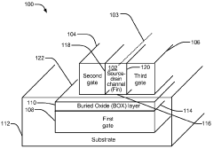
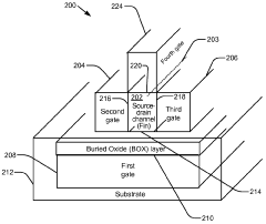
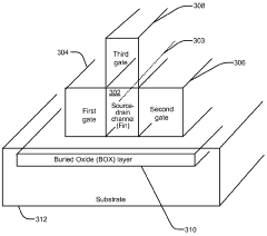
Fin-type device system and method
PatentWO2011028796A1
Innovation
- The use of FinFET transistors with three independently biasable gates, where the first gate is coupled to the fin through a buried oxide layer, allows for lower bias voltage operation during the HOLD phase, thereby increasing the time between memory refreshes and reducing power consumption.
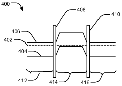
Method of designing fin-based transistor for power optimization
PatentActiveTW201600988A
Innovation
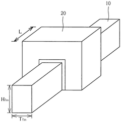
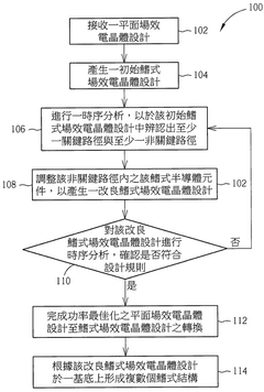
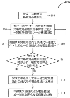
- A method is provided to design a fin structure transistor by identifying critical and non-critical paths in the initial FinFET design through timing analysis, and adjusting fin semiconductor elements in non-critical paths to reduce the number, width, or electrical connections of fins, thereby reducing power consumption.

Process-Voltage-Temperature Variation Management Strategies
Process-Voltage-Temperature (PVT) variations represent significant challenges in FinFET design for low-power applications. These variations can substantially impact device performance, power consumption, and reliability. Effective management strategies must address variations across manufacturing processes, operating voltages, and temperature ranges to ensure optimal device operation.
Process variations stem from manufacturing inconsistencies, resulting in device parameter fluctuations across wafers and dies. Advanced statistical modeling techniques have emerged as essential tools for characterizing these variations. Corner-based analysis remains widely used, but statistical approaches like Statistical Static Timing Analysis (SSTA) provide more comprehensive insights into process variability impacts. Leading foundries now offer Process Design Kits (PDKs) with enhanced statistical models specifically tailored for FinFET technologies.
Voltage variation management has become increasingly critical as supply voltages approach threshold voltages in low-power designs. Adaptive Voltage Scaling (AVS) techniques dynamically adjust supply voltages based on workload and environmental conditions, optimizing power consumption while maintaining performance targets. Recent implementations incorporate on-chip voltage monitors and feedback control systems that can respond to variations in real-time, achieving up to 30% power reduction in modern FinFET designs.
Temperature variations significantly affect FinFET performance characteristics, particularly leakage current which exhibits exponential temperature dependence. Dynamic Thermal Management (DTM) strategies employ temperature sensors distributed across the die to monitor thermal conditions. When hotspots are detected, techniques such as frequency scaling, workload migration, or selective power gating are activated to maintain thermal equilibrium. Advanced DTM implementations now incorporate predictive algorithms that anticipate thermal issues before they become critical.
Integrated PVT management solutions combine multiple variation-aware techniques into cohesive frameworks. Body biasing has proven particularly effective in FinFET technologies, allowing post-manufacturing tuning to compensate for process variations. Forward body bias can enhance performance in critical paths, while reverse body bias reduces leakage in non-critical sections. Multi-corner multi-mode (MCMM) analysis ensures designs remain robust across the entire PVT variation spectrum.
Recent research demonstrates that machine learning approaches can significantly enhance PVT variation management. Neural network models trained on extensive simulation data can predict performance impacts across PVT corners with remarkable accuracy, enabling more efficient optimization strategies. These AI-driven approaches are particularly valuable for complex FinFET designs where traditional analytical methods become computationally prohibitive.
Thermal Management Techniques for FinFET Devices
Thermal management has become a critical aspect of FinFET optimization for low-power applications due to the increased power density and self-heating effects inherent in these three-dimensional transistor structures. As device dimensions continue to shrink below 10nm, the thermal conductivity of materials decreases significantly, exacerbating heat dissipation challenges. This phenomenon, known as phonon boundary scattering, directly impacts device performance and reliability.
Several advanced thermal management techniques have emerged to address these challenges. Silicon-on-insulator (SOI) substrates with embedded heat spreaders have demonstrated up to 15% reduction in peak temperature compared to conventional substrates. These specialized substrates incorporate high thermal conductivity materials like diamond or graphene to efficiently channel heat away from active device regions.
Dynamic thermal management (DTM) systems represent another promising approach, utilizing on-chip temperature sensors coupled with intelligent power management algorithms. These systems can dynamically adjust operating frequencies and supply voltages based on real-time thermal profiles, preventing hotspot formation while maintaining performance targets. Recent implementations have shown power savings of 20-30% in mobile application processors without significant performance degradation.
Novel material integration strategies have also proven effective for thermal optimization. The introduction of high-κ metal gate stacks with optimized thermal boundary resistance has reduced interfacial thermal bottlenecks. Additionally, advanced metallization schemes utilizing copper-graphene composites have improved thermal conductivity in interconnect layers by up to 45% compared to traditional copper interconnects.
Three-dimensional heat spreading techniques have gained traction in recent FinFET designs. Through-silicon vias (TSVs) and microfluidic cooling channels integrated within the chip architecture provide direct thermal pathways to remove heat from critical device regions. Experimental prototypes have demonstrated junction temperature reductions of up to 20°C under full computational loads.
Package-level thermal solutions complement on-chip techniques through advanced thermal interface materials (TIMs) and integrated heat spreaders. Phase-change materials with high thermal conductivity and low thermal resistance have shown particular promise, reducing the thermal resistance between die and package by up to 30% compared to conventional thermal greases.
Computational methods for thermal analysis have also evolved significantly, enabling accurate prediction of thermal profiles during the design phase. Multi-physics simulation tools now incorporate electro-thermal coupling effects, allowing designers to identify and mitigate potential hotspots before fabrication. These predictive capabilities have become essential for optimizing FinFET layouts for thermal performance while maintaining electrical characteristics.
Unlock deeper insights with Patsnap Eureka Quick Research — get a full tech report to explore trends and direct your research. Try now!
Generate Your Research Report Instantly with AI Agent
Supercharge your innovation with Patsnap Eureka AI Agent Platform!