Discover FinFET Applications For Autonomous Vehicles
SEP 11, 202510 MIN READ
Generate Your Research Report Instantly with AI Agent
Patsnap Eureka helps you evaluate technical feasibility & market potential.
FinFET Technology Evolution and Automotive Goals
FinFET technology has evolved significantly since its introduction in the early 2000s, transforming from an experimental transistor design to a cornerstone of modern semiconductor manufacturing. Initially developed to address the limitations of planar transistors at sub-28nm nodes, FinFETs have demonstrated superior performance in power efficiency, reduced leakage current, and enhanced control of short-channel effects. The three-dimensional fin structure allows for better electrostatic control of the channel, enabling continued scaling according to Moore's Law beyond what was possible with traditional transistor architectures.
The evolution trajectory of FinFET technology has seen several key advancements, including the transition from 22nm to 14nm, 10nm, 7nm, and now approaching 5nm and 3nm nodes. Each generation has brought improvements in transistor density, switching speed, and energy efficiency—all critical factors for automotive applications where computational demands are increasing exponentially.
For autonomous vehicles specifically, the technical goals associated with FinFET implementation center around five critical areas: computational performance, power efficiency, reliability, thermal management, and longevity. Autonomous driving systems require massive parallel processing capabilities to handle sensor fusion, real-time decision making, and complex AI algorithms—all while operating within strict power and thermal constraints of a vehicle environment.
The performance-per-watt metrics of advanced FinFET nodes directly address the computational challenges of autonomous driving. Level 4 and 5 autonomy systems are estimated to require processing power exceeding 75 TOPS (Trillion Operations Per Second), which current-generation FinFET-based SoCs are beginning to deliver while maintaining acceptable power envelopes for automotive deployment.
Reliability requirements for automotive semiconductors are particularly stringent, with expected operational lifespans of 10-15 years under extreme temperature conditions (-40°C to 125°C). FinFET technology is evolving to meet these requirements through enhanced electromigration resistance, improved gate oxide reliability, and better resistance to hot carrier injection—all failure mechanisms that become more pronounced in automotive use cases.
The roadmap for FinFET technology in autonomous vehicles is increasingly focused on specialized designs that incorporate redundancy, fault-tolerance, and functional safety features directly at the transistor and circuit design levels. This includes radiation-hardened designs to protect against soft errors that could compromise safety-critical functions in autonomous driving systems.
Looking forward, the convergence of FinFET technology with new materials such as GaN and SiC, along with potential transitions to Gate-All-Around (GAA) architectures, represents the next frontier in meeting the escalating computational demands of fully autonomous vehicles while addressing the stringent power, thermal, and reliability constraints of automotive applications.
Market Demand for Advanced Semiconductors in Autonomous Vehicles
The autonomous vehicle market is witnessing unprecedented growth, driving substantial demand for advanced semiconductor technologies. Market research indicates that the global autonomous vehicle semiconductor market is projected to grow at a CAGR of 36.5% between 2023 and 2030, reaching a valuation of $38.4 billion by 2030. This remarkable growth trajectory is fueled by increasing investments in autonomous driving technologies and the rising integration of advanced driver-assistance systems (ADAS) across various vehicle segments.
FinFET technology, with its superior performance characteristics, has emerged as a critical enabler for autonomous vehicle applications. The demand for FinFET-based semiconductors in this sector is primarily driven by the need for high-performance computing capabilities required to process vast amounts of sensor data in real-time. Autonomous vehicles typically generate between 4TB and 5TB of data per day from various sensors including LiDAR, radar, cameras, and ultrasonic sensors, necessitating powerful processing solutions.
Industry analysis reveals that Level 3 to Level 5 autonomous vehicles require 2-3 times more semiconductor content compared to conventional vehicles. This increased semiconductor intensity is particularly evident in the computing platforms, where FinFET-based processors are becoming the standard due to their superior power efficiency and performance density. The market for these advanced computing platforms in autonomous vehicles is expected to grow at 42% annually through 2028.
Regional market assessment shows North America and Asia-Pacific leading the demand for advanced semiconductors in autonomous vehicles. China, in particular, has set ambitious targets for autonomous vehicle adoption, with plans to have 20% of new vehicles sold with at least Level 3 autonomy by 2025, creating substantial demand for FinFET-based solutions.
Consumer and regulatory trends are further accelerating market growth. Safety regulations in major markets are increasingly mandating advanced driver assistance features, many of which require high-performance computing capabilities that benefit from FinFET technology. Additionally, consumer expectations for enhanced in-vehicle experiences and connectivity features are driving demand for more sophisticated semiconductor solutions.
Supply chain considerations are becoming increasingly critical in this market. Recent semiconductor shortages have highlighted the strategic importance of securing advanced semiconductor manufacturing capacity. This has led to significant investments in semiconductor manufacturing infrastructure globally, with particular emphasis on advanced node technologies including FinFET processes at 7nm and below.
FinFET Current State and Implementation Challenges
FinFET technology has reached a mature state in semiconductor manufacturing, with widespread adoption in high-performance computing applications. Current implementations typically feature gate lengths ranging from 22nm down to 5nm in the most advanced commercial processes. The multi-gate transistor architecture of FinFETs provides superior electrostatic control over the channel, resulting in reduced leakage current and improved power efficiency compared to planar transistors. This makes them particularly valuable for autonomous vehicle applications where both computational performance and power constraints are critical considerations.
Despite their advantages, FinFET implementation faces several significant challenges when targeting autonomous vehicle systems. Thermal management remains a primary concern, as the three-dimensional structure of FinFETs creates higher power density and localized heating issues. This is especially problematic in automotive environments where ambient temperatures can vary dramatically and cooling solutions must be robust against vibration and long-term reliability requirements.
Manufacturing complexity presents another major hurdle. The intricate three-dimensional fin structures require sophisticated lithography and etching processes that increase production costs and yield challenges. For automotive-grade chips that demand zero-defect manufacturing, these complexities are magnified by the need for extended qualification processes and adherence to functional safety standards such as ISO 26262.
Variability in device characteristics poses additional challenges for autonomous vehicle applications. Process variations in fin height, width, and shape can lead to inconsistent performance across chips, potentially affecting the deterministic behavior required for safety-critical functions. This variability becomes increasingly problematic as FinFET dimensions shrink below 7nm, where quantum effects begin to dominate device physics.
Radiation hardness represents a growing concern for FinFET deployment in autonomous vehicles. As these vehicles incorporate more advanced driver assistance systems and move toward full autonomy, their susceptibility to single-event upsets from cosmic radiation increases. The reduced node size of modern FinFETs makes them potentially more vulnerable to such effects, necessitating additional design considerations for fault tolerance and error detection.
Power management challenges are particularly relevant for electric and hybrid autonomous vehicles. While FinFETs offer improved power characteristics compared to older technologies, the massive computational requirements of autonomous systems demand further optimization. Dynamic voltage and frequency scaling must be carefully implemented to balance performance needs with battery life considerations, especially for edge AI processing that cannot rely on cloud connectivity.
Integration with analog and mixed-signal components presents another implementation challenge. Autonomous vehicles require numerous sensors with analog interfaces that must coexist with digital processing on the same chip. The process optimizations for FinFET digital performance sometimes compromise analog device characteristics, creating design trade-offs that impact overall system performance.
Current FinFET Solutions for Autonomous Vehicle Applications
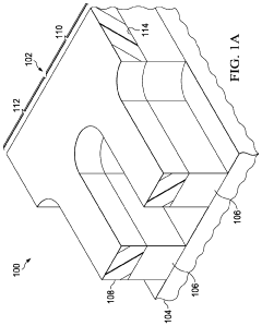
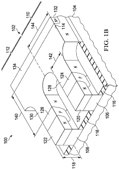
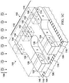
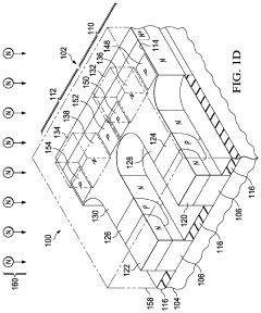
01 FinFET structure and fabrication methods
FinFET devices feature a three-dimensional structure where the gate wraps around a thin silicon fin that forms the channel. This design allows for better control of the channel, reducing short-channel effects and improving performance. The fabrication methods include creating silicon fins on a substrate, depositing gate materials around these fins, and implementing various doping techniques to achieve desired electrical characteristics.- FinFET structure and fabrication methods: FinFET devices feature a three-dimensional structure where the gate wraps around a thin silicon fin that forms the channel. This design allows for better control of the channel, reducing short-channel effects and improving performance. The fabrication process typically involves forming silicon fins on a substrate, depositing gate materials around these fins, and implementing various doping techniques to create source and drain regions.
- Multi-gate FinFET configurations: Multi-gate FinFET designs enhance transistor performance by providing better electrostatic control of the channel. These configurations include double-gate, tri-gate, and gate-all-around structures, each offering progressive improvements in controlling leakage current and short-channel effects. The multiple gate approach allows for scaling to smaller technology nodes while maintaining or improving performance characteristics.
- FinFET design optimization techniques: Various techniques are employed to optimize FinFET designs, including fin pitch scaling, fin height adjustments, and work function engineering. These optimizations aim to balance performance, power consumption, and area efficiency. Advanced simulation tools help predict device behavior and allow for iterative improvements before physical implementation, reducing development cycles and improving yield.
- FinFET integration with other semiconductor technologies: FinFETs can be integrated with various semiconductor technologies to create hybrid solutions that leverage the advantages of each approach. This includes integration with conventional planar CMOS, SOI (Silicon-On-Insulator) technology, and various memory architectures. The integration enables the development of high-performance, low-power system-on-chip solutions for diverse applications ranging from mobile devices to high-performance computing.
- Advanced FinFET applications and future developments: FinFET technology enables advanced applications in high-performance computing, artificial intelligence, and mobile devices. Ongoing developments include vertical FinFETs, nanosheet/nanowire transistors as FinFET successors, and integration with novel materials like III-V semiconductors. These advancements aim to extend Moore's Law beyond traditional scaling limits, offering pathways to continue improving semiconductor performance while managing power consumption and manufacturing complexity.
02 Multi-gate FinFET configurations
Multi-gate FinFET designs involve implementing multiple gates around the silicon fin to enhance control over the channel. These configurations include double-gate, tri-gate, and gate-all-around structures, each offering different levels of electrostatic control and performance characteristics. The multi-gate approach helps minimize leakage current and improve the transistor's on/off ratio, making it suitable for advanced semiconductor applications.Expand Specific Solutions03 FinFET design optimization and simulation
Design optimization and simulation techniques are crucial for developing efficient FinFET devices. This includes computational modeling to predict device performance, optimize fin dimensions, gate length, and spacing. Advanced simulation tools help engineers analyze electrical characteristics, thermal behavior, and reliability factors before physical fabrication, reducing development cycles and improving yield rates.Expand Specific Solutions04 FinFET integration with other semiconductor technologies
Integration of FinFET technology with other semiconductor processes and structures enhances overall system performance. This includes combining FinFETs with conventional planar transistors, implementing them in system-on-chip designs, and integrating with memory technologies. The integration approaches address challenges related to mixed-signal applications, power management, and compatibility with existing manufacturing processes.Expand Specific Solutions05 Advanced FinFET materials and scaling techniques
Research into novel materials and scaling techniques aims to extend FinFET technology beyond traditional silicon implementations. This includes exploring high-mobility channel materials like germanium and III-V compounds, implementing strain engineering to enhance carrier mobility, and developing vertical fin structures to increase density. These advancements address challenges in continued device scaling while maintaining or improving performance metrics.Expand Specific Solutions
Key Semiconductor Players in Automotive FinFET Market
The FinFET technology market for autonomous vehicles is in its growth phase, with increasing adoption driven by demands for high-performance, energy-efficient computing in advanced driver-assistance systems. Major semiconductor manufacturers including TSMC, GlobalFoundries, and SMIC are competing to develop specialized FinFET solutions that meet the stringent requirements of automotive applications. The market is characterized by technological differentiation, with companies like NXP, STMicroelectronics, and Infineon focusing on automotive-grade FinFET implementations that ensure reliability and safety compliance. Apple and IBM are leveraging their expertise in chip design to influence the ecosystem. The technology is approaching maturity for automotive applications, with established players investing in specialized manufacturing processes while emerging competitors from China are rapidly advancing their capabilities to challenge market leaders.
Taiwan Semiconductor Manufacturing Co., Ltd.
Technical Solution: TSMC has pioneered advanced FinFET technology specifically optimized for autonomous vehicle applications. Their 7nm and 5nm FinFET processes deliver high-performance computing capabilities essential for AI processing in autonomous driving systems. TSMC's automotive-grade FinFET technology incorporates enhanced reliability features including extended temperature range operation (-40°C to 150°C), stringent AEC-Q100 qualification, and specialized fault-tolerance mechanisms. Their N5A process technology, built on their 5nm FinFET platform, is specifically designed for automotive applications with 20% faster processing speeds compared to their 7nm technology while consuming 40% less power. This enables complex real-time decision-making algorithms required for autonomous navigation while meeting the strict power and thermal constraints of automotive environments. TSMC also implements specialized ESD protection and latch-up immunity in their automotive FinFET designs to ensure resilience against electrical disturbances common in vehicle environments.
Strengths: Industry-leading process node advancement (down to 3nm), extensive automotive qualification experience, and superior power efficiency. Weaknesses: Higher manufacturing costs compared to older process nodes and potential supply chain constraints during high demand periods.
International Business Machines Corp.
Technical Solution: IBM has developed specialized FinFET architectures optimized for autonomous vehicle applications, focusing on their cognitive computing capabilities. Their automotive-grade FinFET technology integrates with their AI accelerator designs to enable efficient neural network processing for autonomous driving functions. IBM's approach combines their silicon-on-insulator (SOI) FinFET technology with specialized circuit designs that enhance reliability under automotive conditions. Their FinFET implementations feature radiation-hardened designs that provide up to 30% better soft error resilience compared to conventional approaches, critical for maintaining system integrity in autonomous driving scenarios. IBM has also pioneered vertical transport field effect transistors (VTFETs) as an evolution of FinFET technology, which can potentially deliver 2x improvement in performance or 85% reduction in energy consumption - particularly valuable for the power-constrained environments of electric autonomous vehicles. Their FinFET designs incorporate specialized ECC (Error Correction Code) capabilities at the hardware level to ensure computational accuracy for safety-critical autonomous functions.
Strengths: Superior integration with AI acceleration technologies and extensive experience in reliability engineering for mission-critical applications. Weaknesses: Less focused on high-volume manufacturing compared to pure-play foundries, potentially limiting widespread adoption in automotive markets.
Core FinFET Patents and Technical Innovations
Transistor device and method of manufacturing such a transistor device
PatentInactiveEP2122687A1
Innovation
- A transistor device and manufacturing method that incorporates a fin structure with alternating source/drain regions of different conductivities and a dual gate structure, combining FinFET and TFET technologies to reduce area occupation and enhance performance, allowing for both N-type and P-type tunneling field effect transistors in a single fin.
finFET with lateral charge balance at the drain drift region
PatentActiveUS11916142B2
Innovation
- The introduction of an extended drain finFET design, which includes a drain drift region with an enhanced portion and charge balance regions, allowing for a higher net average conductivity type dopant concentration and enabling operation at higher drain potentials by concentrating current flow and reducing resistance.
Thermal Management and Reliability in Automotive FinFETs
The thermal management of FinFET technology in autonomous vehicles presents unique challenges due to the extreme operating conditions and reliability requirements of automotive environments. FinFETs in autonomous driving systems must maintain stable performance across temperature ranges from -40°C to 150°C, significantly more demanding than consumer electronics applications. The compact three-dimensional structure of FinFETs, while beneficial for performance, creates thermal hotspots that can accelerate device degradation if not properly managed.
Automotive-grade FinFETs implement specialized thermal dissipation techniques including advanced packaging with improved thermal interface materials (TIMs) and integrated heat spreaders designed specifically for vehicular applications. These components must maintain thermal conductivity over the 10-15 year expected lifespan of vehicles, far exceeding consumer electronics requirements.
Reliability testing for automotive FinFETs follows the AEC-Q100 qualification standard, with particular emphasis on Grade 1 requirements for engine control applications. This includes extended temperature cycling, humidity testing, and electrostatic discharge (ESD) resilience beyond standard semiconductor testing protocols. Manufacturers have developed specialized burn-in procedures that simulate years of thermal cycling to identify potential early failures.
Dynamic thermal management systems in autonomous vehicles continuously monitor FinFET junction temperatures and adjust processing loads accordingly. Advanced algorithms predict thermal conditions based on workload patterns and environmental factors, preemptively scaling frequency or redistributing computational tasks before thermal thresholds are reached. This predictive approach is critical for maintaining consistent performance in safety-critical autonomous driving functions.
Radiation hardening represents another crucial aspect of automotive FinFET reliability. As process nodes shrink below 10nm, sensitivity to cosmic radiation increases, potentially causing single-event upsets (SEUs) that could compromise autonomous driving systems. Manufacturers implement redundant circuit designs and error-correction techniques specifically calibrated for automotive radiation profiles at various altitudes and geographic locations.
The industry is advancing toward heterogeneous integration approaches that combine FinFET processing cores with specialized accelerators using 2.5D and 3D packaging. These architectures distribute thermal loads more effectively while providing computational redundancy. Emerging liquid cooling solutions designed specifically for automotive electronics promise to further enhance thermal management capabilities, potentially enabling higher performance FinFET implementations in next-generation autonomous vehicles.
Safety Standards and Certification for Automotive Semiconductors
The integration of FinFET technology in autonomous vehicle applications necessitates adherence to stringent safety standards and certification processes for automotive semiconductors. The automotive industry operates under comprehensive regulatory frameworks that ensure electronic components can withstand harsh operating conditions while maintaining functional safety throughout the vehicle's lifecycle.
ISO 26262, the international standard for functional safety of electrical and electronic systems in production automobiles, serves as the cornerstone for semiconductor qualification in autonomous vehicles. This standard defines Automotive Safety Integrity Levels (ASIL), ranging from A to D, with ASIL D representing the highest safety requirements. FinFET-based processors and SoCs for autonomous driving functions typically require ASIL C or D certification, demanding extensive verification, validation, and documentation processes.
Beyond ISO 26262, the AEC-Q100 qualification standard specifically addresses stress test qualification for integrated circuits in automotive applications. FinFET semiconductors must undergo rigorous temperature cycling, electrostatic discharge testing, and reliability assessments to achieve AEC-Q100 Grade 1 certification, which validates operation in the extended temperature range of -40°C to +125°C essential for automotive environments.
The emergence of autonomous driving has prompted the development of new standards addressing AI and machine learning components. The SOTIF (Safety Of The Intended Functionality) standard, defined in ISO/PAS 21448, complements ISO 26262 by addressing safety challenges arising from functional insufficiencies and foreseeable misuse rather than system failures. This is particularly relevant for FinFET-based neural processing units that power perception systems in autonomous vehicles.
Cybersecurity certification has become increasingly critical as autonomous vehicles incorporate more connected features. The UN Regulation No. 155 on Cyber Security and Security Management System and ISO/SAE 21434 establish requirements for managing cybersecurity risks in automotive electronic systems, including semiconductor hardware security features that FinFET technology must incorporate.
Certification processes for automotive FinFET semiconductors involve extensive documentation, including Failure Mode and Effects Analysis (FMEA), fault tree analysis, and hardware-software interface specifications. Manufacturers must implement robust development processes with traceability throughout the product lifecycle and demonstrate systematic capability through assessments by independent certification bodies.
The trend toward autonomous driving is driving evolution in safety standards, with emerging frameworks addressing specific challenges of AI-based systems. These include runtime monitoring requirements, verification methodologies for neural networks, and standards for hardware acceleration of safety-critical AI workloads—all areas where FinFET technology plays a crucial enabling role.
Unlock deeper insights with Patsnap Eureka Quick Research — get a full tech report to explore trends and direct your research. Try now!
Generate Your Research Report Instantly with AI Agent
Supercharge your innovation with Patsnap Eureka AI Agent Platform!