

Optimizing FinFET Gate Length For Enhanced Performance
SEP 11, 20259 MIN READ
Generate Your Research Report Instantly with AI Agent
PatSnap Eureka helps you evaluate technical feasibility & market potential.
FinFET Evolution and Performance Objectives
The evolution of FinFET technology represents one of the most significant advancements in semiconductor manufacturing over the past two decades. Initially introduced by researchers at the University of California, Berkeley in 1998, FinFETs emerged as a revolutionary solution to the scaling limitations of traditional planar transistors. The three-dimensional fin structure allowed for superior electrostatic control of the channel, effectively addressing short-channel effects that had begun to plague conventional MOSFET designs as dimensions shrank below 28nm.
The technology progressed through several critical phases, beginning with early research demonstrations, followed by industry adoption around the 22nm node by Intel in 2011, and subsequent refinement by other major semiconductor manufacturers. Each generation has seen systematic improvements in fin geometry, gate stack materials, and process integration techniques, all aimed at enhancing performance while managing power consumption.
Gate length optimization has consistently been a central focus in FinFET development. As transistors scaled down, the relationship between gate length and device performance became increasingly complex. Shorter gate lengths enable faster switching speeds and higher drive currents, directly impacting computational performance. However, excessive reduction introduces severe short-channel effects, including drain-induced barrier lowering (DIBL) and threshold voltage roll-off, which compromise reliability and increase leakage current.
The industry has established several key performance objectives for FinFET optimization. Primary among these is achieving the optimal balance between switching speed and power efficiency—a critical consideration for both high-performance computing and mobile applications. Secondary objectives include enhancing reliability through improved thermal characteristics, reducing variability in manufacturing, and ensuring compatibility with existing CMOS process flows.
Recent technological trends indicate a move toward gate lengths in the range of 10-20nm for leading-edge nodes, with sophisticated engineering solutions implemented to maintain electrostatic integrity. These include high-k metal gate stacks, strain engineering, and precise fin profile control. The trajectory suggests continued scaling toward sub-10nm gate lengths, though with increasing reliance on complementary innovations in materials and process technology.
The ultimate goal of gate length optimization extends beyond simple dimensional scaling to encompass a holistic approach to transistor design. This includes consideration of the entire device architecture, including fin height-to-width ratio, gate-to-source/drain spacing, and the implementation of novel contact schemes to minimize parasitic resistances that become increasingly dominant at smaller dimensions.
Market Demand for Advanced Semiconductor Nodes
The semiconductor industry is experiencing unprecedented demand for advanced nodes, driven primarily by the proliferation of high-performance computing applications, artificial intelligence, and 5G technologies. Market research indicates that the global semiconductor market is projected to reach $1 trillion by 2030, with advanced nodes below 7nm accounting for approximately 35% of this value. This growth trajectory underscores the critical importance of FinFET technology optimization, particularly gate length engineering.
Consumer electronics continues to be the largest market segment demanding advanced semiconductor nodes, with smartphones and tablets requiring increasingly powerful yet energy-efficient processors. The smartphone market alone consumes over 30% of all advanced node semiconductors produced globally, with manufacturers constantly pushing for smaller form factors and extended battery life that only optimized FinFETs can deliver.
Data centers represent another rapidly expanding market segment, with annual growth rates exceeding 15% as cloud computing services expand. These facilities require processors that balance computational power with energy efficiency, making optimized FinFET gate length a critical parameter. The total cost of ownership calculations for data centers heavily weight power consumption, creating strong economic incentives for semiconductor advancements that reduce power requirements while maintaining performance.
Automotive electronics has emerged as a significant new market driver, with the average semiconductor content in vehicles increasing by approximately 12% annually. Advanced driver assistance systems (ADAS) and autonomous driving capabilities demand high-performance, low-latency processing that only advanced nodes can provide. The automotive sector's stringent reliability requirements also place additional emphasis on optimized gate length to ensure consistent performance across temperature ranges and operating conditions.
The artificial intelligence and machine learning sector represents perhaps the most aggressive growth area for advanced semiconductor demand. Training large AI models requires massive computational resources, with major AI research organizations increasing their semiconductor procurement budgets by over 200% in the past three years. This sector specifically benefits from optimized FinFET gate length that enables higher transistor density and improved performance per watt metrics.
Geographically, East Asia dominates semiconductor demand, accounting for over 60% of advanced node consumption, followed by North America at approximately 25%. However, recent geopolitical tensions have accelerated efforts to diversify the semiconductor supply chain, with significant investments in new fabrication facilities across Europe and North America, all of which will require cutting-edge FinFET technology with optimized gate length parameters to remain competitive.
Current FinFET Gate Length Challenges
The semiconductor industry's relentless pursuit of performance enhancement has led to significant challenges in FinFET gate length optimization. Current FinFET technology faces several critical limitations as manufacturers attempt to scale gate lengths below 10nm. Short channel effects (SCEs) become increasingly pronounced at these dimensions, causing threshold voltage roll-off, drain-induced barrier lowering (DIBL), and increased subthreshold swing, all of which compromise device performance and power efficiency.
Manufacturing precision presents another substantial challenge. As gate lengths shrink, process variations become proportionally more significant, leading to inconsistent device characteristics across chips. Even minor variations of 1-2nm can cause substantial performance differences when working with gate lengths in the 10-20nm range, significantly impacting yield rates and reliability metrics.
Quantum mechanical effects emerge as dominant factors at ultra-short gate lengths. Electron tunneling through the potential barrier becomes more probable, resulting in increased leakage currents that undermine the power efficiency advantages that FinFETs initially promised. These quantum effects fundamentally alter device behavior in ways that traditional scaling models fail to predict accurately.
Heat dissipation represents an increasingly critical constraint as gate lengths decrease. The power density within these nanoscale structures rises dramatically, creating thermal hotspots that can degrade performance, reliability, and device lifespan. Current thermal management solutions struggle to efficiently extract heat from these densely packed three-dimensional structures.
Material limitations further complicate optimization efforts. High-k dielectric materials and metal gates, while essential for reducing leakage, introduce interface quality challenges that affect carrier mobility. Additionally, the fin material itself faces strain and defect issues at extremely small dimensions, potentially compromising the structural integrity of the device.
Parasitic capacitance and resistance effects become increasingly dominant as gate lengths shrink. The relative contribution of contact resistance and fringe capacitance grows disproportionately, offsetting the performance gains expected from scaling. Industry data suggests that parasitic components can account for over 70% of total resistance in advanced FinFET nodes.
Balancing these technical challenges with economic considerations presents a complex optimization problem. The cost of manufacturing equipment capable of precisely controlling sub-10nm features increases exponentially, while yield challenges further impact production economics. This has led to a slowdown in gate length scaling across the industry, with manufacturers exploring alternative approaches such as multi-gate architectures, vertical arrangements, and novel channel materials.
Gate Length Optimization Techniques
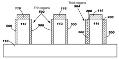
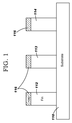
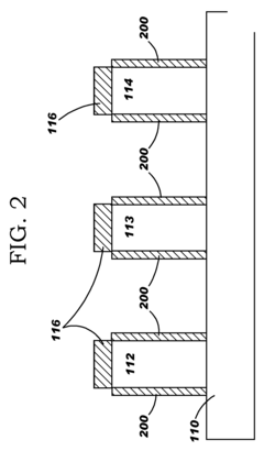
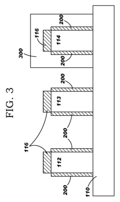
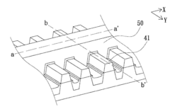
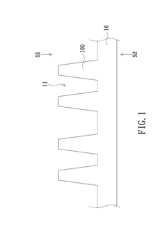
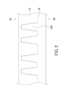
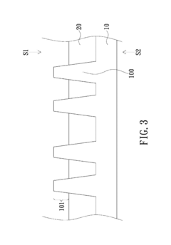
01 Gate length scaling in FinFET devices
FinFET technology allows for scaling of gate lengths to smaller dimensions compared to traditional planar transistors. This scaling enables higher performance and lower power consumption in semiconductor devices. Various techniques are employed to achieve shorter gate lengths while maintaining device reliability and performance characteristics. The reduced gate length in FinFETs helps to minimize short-channel effects and improve electrostatic control of the channel.- Gate length scaling in FinFET devices: FinFET technology allows for effective scaling of gate lengths to smaller dimensions compared to traditional planar transistors. This scaling enables higher performance and lower power consumption in semiconductor devices. Various techniques are employed to achieve gate lengths in the nanometer range while maintaining good electrostatic control and minimizing short-channel effects. The fin structure provides better control of the channel, allowing for shorter gate lengths without significant leakage current increases.
- Multi-gate FinFET structures with varying gate lengths: Multi-gate FinFET designs incorporate different gate lengths within the same device or across different devices on a chip. This approach allows for optimization of performance characteristics such as switching speed, leakage current, and power consumption. By implementing varying gate lengths, manufacturers can create devices with different threshold voltages and performance characteristics on the same substrate, enabling more versatile and efficient integrated circuit designs.
- Gate length control methods in FinFET fabrication: Precise control of gate length in FinFET fabrication is critical for device performance and consistency. Various methods are employed to achieve accurate gate length control, including advanced lithography techniques, spacer-defined gate processes, and selective etching procedures. These methods help maintain uniform gate lengths across the wafer and reduce variations that could affect device performance. Techniques such as sidewall image transfer and self-aligned double patterning are particularly useful for achieving sub-lithographic gate lengths.
- Gate length effects on FinFET performance characteristics: The gate length of a FinFET significantly impacts its performance characteristics, including threshold voltage, on-current, off-current, and switching speed. Shorter gate lengths generally result in faster switching speeds but may increase leakage current and short-channel effects. Optimizing gate length is essential for balancing performance requirements with power consumption constraints. The relationship between gate length and other device parameters, such as fin width and height, must be carefully considered to achieve desired device characteristics.
- Advanced FinFET architectures with specialized gate length configurations: Advanced FinFET architectures incorporate specialized gate length configurations to address specific performance requirements. These include gate-all-around structures, omega-shaped gates, and asymmetric gate designs. Such architectures may feature non-uniform gate lengths along the fin height or width to optimize carrier transport and electrostatic control. These specialized configurations enable further improvements in device performance, power efficiency, and scaling capabilities beyond conventional FinFET designs.
02 Multi-gate FinFET structures with varying gate lengths
Multi-gate FinFET structures can be designed with different gate lengths to optimize device performance for specific applications. By implementing varying gate lengths in the same device or across different devices on a chip, manufacturers can balance performance, power consumption, and area requirements. This approach allows for customization of threshold voltages and other electrical characteristics without requiring additional process steps.Expand Specific Solutions03 Gate length control techniques in FinFET fabrication
Precise control of gate length is critical in FinFET manufacturing. Various techniques are employed to achieve accurate and consistent gate lengths, including advanced lithography methods, sidewall spacer technology, and selective etching processes. These techniques help to minimize variations in gate length across the wafer and ensure uniform device performance. The control of gate length directly impacts key device parameters such as threshold voltage, drive current, and leakage current.Expand Specific Solutions04 Gate length effects on FinFET performance and reliability
The gate length of FinFETs significantly affects device performance and reliability. Shorter gate lengths generally lead to higher drive currents and faster switching speeds but may also increase leakage current and susceptibility to short-channel effects. Optimizing gate length involves balancing these trade-offs to meet specific performance requirements while ensuring long-term device reliability. Gate length also influences hot carrier injection, bias temperature instability, and other reliability concerns in FinFET devices.Expand Specific Solutions05 Advanced FinFET architectures with novel gate length designs
Novel FinFET architectures incorporate innovative gate length designs to enhance performance and functionality. These include asymmetric gate structures, gate-all-around configurations, and vertically stacked nanowire/nanosheet transistors. Such advanced designs enable further scaling of semiconductor devices while addressing challenges related to power consumption and device density. These architectures often employ sophisticated gate engineering techniques to optimize carrier transport and electrostatic control in the channel region.Expand Specific Solutions
Leading Semiconductor Manufacturers Analysis
The FinFET gate length optimization landscape is currently in a mature growth phase, with the global semiconductor market for advanced nodes exceeding $60 billion annually. Technology maturity varies significantly among key players, with TSMC, Samsung, and Intel leading the field through their established sub-10nm FinFET processes. AMD and GlobalFoundries maintain competitive positions through strategic partnerships, while SMIC and UMC are rapidly advancing their capabilities. Chinese players like YMTC and ChangXin Memory are investing heavily to close the technology gap. The competitive dynamics are intensifying as companies like IBM and Tokyo Electron contribute breakthrough research in gate engineering techniques, driving the industry toward atomic-scale precision in gate length control to maximize performance while managing power consumption.
Advanced Micro Devices, Inc.
Technical Solution: AMD, working closely with manufacturing partners, has implemented a sophisticated FinFET gate length optimization strategy for their Zen architecture processors. Their approach focuses on balancing performance and power efficiency through careful gate dimension control. AMD utilizes a combination of gate length scaling and work function engineering to achieve optimal threshold voltages for different transistor types across their SoCs. Their methodology incorporates selective strain engineering techniques that complement specific gate length targets for NMOS and PMOS devices. AMD has developed specialized circuit design techniques that account for gate length variations, including adaptive body biasing and dynamic voltage scaling. Their optimization process includes extensive statistical modeling to determine ideal gate length distributions for different functional blocks within their processors. AMD employs gate-last process flows that allow for more precise work function metal deposition and better control of effective gate lengths[4][6]. Their approach also includes specialized power gating architectures that leverage optimized gate dimensions to minimize leakage in standby modes.
Strengths: Excellent balance between performance and power efficiency; sophisticated design-technology co-optimization approach; robust tolerance to process variations. Weaknesses: Reliance on foundry partners for manufacturing process development; potential time-to-market delays when transitioning to new process nodes; challenges in maintaining consistent performance across different manufacturing locations.
GlobalFoundries U.S., Inc.
Technical Solution: GlobalFoundries has developed a differentiated approach to FinFET gate length optimization focused on their 12nm and 14nm FinFET platforms. Their strategy emphasizes reliability and manufacturability while maintaining competitive performance metrics. GlobalFoundries employs a gate-first process with carefully engineered high-k dielectrics and metal gates to achieve target threshold voltages with minimal variation. Their gate length optimization includes specialized etch processes that maintain consistent critical dimensions across wafers. GlobalFoundries has implemented unique strain engineering techniques that work in concert with their gate length targets to enhance carrier mobility. Their approach incorporates multi-layer work function metals that enable precise threshold voltage tuning for different transistor types. GlobalFoundries utilizes advanced optical proximity correction and resolution enhancement techniques to achieve consistent gate patterning[7][8]. Their process includes specialized annealing sequences that minimize diffusion and maintain sharp dopant profiles at the gate edges. GlobalFoundries has also developed specialized electromigration-resistant contact schemes that complement their gate architecture to ensure long-term reliability.
Strengths: Excellent manufacturing consistency and yield; strong reliability performance under various operating conditions; good balance of performance and cost. Weaknesses: Less aggressive dimensional scaling compared to leading-edge competitors; higher power consumption at equivalent performance points; limited ability to support the most demanding high-performance applications.
Critical Patents in FinFET Gate Engineering
Multiple dielectric finfet structure and method
PatentInactiveUS20070290250A1
Innovation
- A method of forming FinFETs with multiple gate dielectric thicknesses by patterning fins, applying a first gate dielectric, protecting some fins with a mask, removing it from others, and adding additional dielectric layers to achieve varying thicknesses, allowing for optimized performance and reliability across different regions.
Fin field effect transistor device and fabrication method thereof
PatentActiveUS20160163837A1
Innovation
- A method for fabricating a FinFET device involving the formation of a substrate with a fin structure, an oxide layer, shallow trench isolation, spacers, and an epitaxial fin structure, where the gate structure is perpendicular to the epitaxial fin, and the epitaxial fin can be made of germanium with varying compositions, allowing for improved electrical control and efficiency.
Thermal Management Considerations
Thermal management has emerged as a critical consideration in FinFET gate length optimization, particularly as device dimensions continue to shrink while power densities increase. The three-dimensional fin structure of FinFETs, while offering superior electrostatic control, creates unique thermal challenges that must be addressed to ensure optimal device performance and reliability. As gate lengths are reduced to enhance performance, the resulting increase in power density can lead to significant self-heating effects that degrade device characteristics.
The thermal conductivity of the fin material plays a crucial role in heat dissipation. Silicon fins typically exhibit reduced thermal conductivity compared to bulk silicon due to phonon boundary scattering effects, which become more pronounced as fin dimensions decrease. This phenomenon creates a thermal bottleneck that can lead to localized hotspots, particularly at the channel region where current densities are highest. Studies have shown that temperature increases of 50-100°C above ambient can occur during normal operation of aggressively scaled FinFETs.
Gate length optimization must therefore consider the trade-off between performance enhancement and thermal management. Shorter gate lengths reduce parasitic capacitance and increase drive current, but simultaneously increase power density and self-heating. Thermal simulations indicate that reducing gate length below certain technology-specific thresholds (typically in the 10-14nm range for current-generation FinFETs) yields diminishing performance returns due to thermal limitations.
Advanced cooling solutions and thermally-aware design methodologies have become essential components of FinFET optimization strategies. These include the integration of high thermal conductivity materials in the gate stack, optimization of fin geometry to enhance heat spreading, and implementation of dynamic thermal management techniques at the circuit level. Some manufacturers have explored the use of alternative channel materials with superior thermal properties, such as silicon-germanium alloys or III-V semiconductors.
The impact of thermal effects on reliability must also be considered when optimizing gate length. Elevated operating temperatures accelerate various degradation mechanisms, including bias temperature instability (BTI), hot carrier injection (HCI), and time-dependent dielectric breakdown (TDDB). These reliability concerns become more pronounced at shorter gate lengths due to increased electric fields and current densities, potentially offsetting the performance benefits of gate length reduction.
Accurate thermal modeling has become indispensable for gate length optimization. Advanced multi-physics simulation tools that couple electrical and thermal effects are now routinely employed to predict device behavior under realistic operating conditions. These simulations enable designers to identify the optimal gate length that balances performance enhancement with thermal constraints for specific application requirements.
Supply Chain Dependencies
The optimization of FinFET gate length is critically dependent on a complex global supply chain that encompasses raw materials, specialized manufacturing equipment, and advanced fabrication facilities. Silicon wafer production, the foundation of FinFET manufacturing, relies heavily on a few key suppliers primarily located in Japan, Germany, and the United States. Any disruption in this segment can significantly impact the entire semiconductor industry's ability to innovate in gate length optimization.
Lithography equipment, essential for defining precise gate lengths, represents another critical dependency. ASML, based in the Netherlands, maintains a near-monopoly on extreme ultraviolet (EUV) lithography systems required for sub-7nm node fabrication where advanced gate length optimization occurs. This concentration creates a potential bottleneck, as delivery times for these sophisticated machines can exceed 18 months and costs approach $150 million per unit.
Chemical suppliers constitute another vital link in the chain, providing the specialized etching chemicals and high-purity materials necessary for gate formation. The production of these chemicals is concentrated among a small number of companies in Japan, Germany, and the United States, creating vulnerability to regional disruptions or trade restrictions.
Intellectual property dependencies further complicate the landscape. Key patents related to FinFET gate optimization are held by major semiconductor companies and research institutions across the United States, Taiwan, South Korea, and increasingly China. Cross-licensing agreements have become essential for manufacturers seeking to implement the most effective gate length optimization techniques.
Geopolitical tensions have heightened awareness of these supply chain vulnerabilities. Recent initiatives in the United States, European Union, and East Asia aim to strengthen domestic semiconductor manufacturing capabilities, including the specialized processes required for advanced FinFET production. However, complete supply chain localization remains economically unfeasible due to the specialized nature of many components.
Talent availability represents a final critical dependency. The highly specialized engineering expertise required for gate length optimization is concentrated in specific geographic clusters, primarily in the United States, Taiwan, and South Korea. Companies must navigate global competition for this limited talent pool while addressing immigration and work visa challenges that can restrict access to international expertise.
Unlock deeper insights with PatSnap Eureka Quick Research — get a full tech report to explore trends and direct your research. Try now!
Generate Your Research Report Instantly with AI Agent
Supercharge your innovation with PatSnap Eureka AI Agent Platform!