

Measure FinFET Threshold Voltage Shift Using Method X
SEP 11, 20259 MIN READ
Generate Your Research Report Instantly with AI Agent
PatSnap Eureka helps you evaluate technical feasibility & market potential.
FinFET Threshold Voltage Measurement Background and Objectives
FinFET technology has revolutionized semiconductor manufacturing since its introduction in the early 2000s, offering superior electrostatic control and reduced short-channel effects compared to planar transistors. The evolution of this technology has been marked by continuous miniaturization, with current commercial nodes reaching 5nm and below. This progression has intensified the importance of precise threshold voltage (Vth) measurement and control, as even minor shifts can significantly impact device performance and power consumption.
The threshold voltage in FinFETs represents the gate voltage required to create a conducting channel between source and drain. Unlike planar devices, the three-dimensional fin structure introduces unique challenges for Vth measurement due to quantum confinement effects, fin geometry variations, and complex electrostatics at the nanoscale. Traditional measurement techniques developed for planar technologies often prove inadequate for capturing the nuanced behavior of FinFET devices.
Method X emerges as a novel approach for measuring threshold voltage shifts in FinFETs with enhanced precision. This technique addresses the limitations of conventional methods by incorporating advanced sensing mechanisms that account for the three-dimensional nature of the channel. The primary objective of investigating Method X is to establish a reliable, high-throughput measurement protocol that can detect subtle Vth variations across different operating conditions and aging states.
Accurate threshold voltage measurement is particularly critical as FinFET technology matures and faces reliability challenges such as bias temperature instability (BTI), hot carrier injection (HCI), and time-dependent dielectric breakdown (TDDB). These phenomena cause gradual shifts in threshold voltage over time, potentially leading to circuit malfunction or premature device failure. Method X aims to provide early detection capabilities for these reliability issues, enabling more effective device optimization and lifetime prediction.
The technical goals of this investigation include quantifying the sensitivity and repeatability of Method X compared to established techniques, determining its applicability across different FinFET architectures (including various fin widths, heights, and gate lengths), and evaluating its potential for integration into high-volume manufacturing test flows. Additionally, we seek to establish correlations between measured Vth shifts and specific degradation mechanisms, thereby enhancing our fundamental understanding of FinFET reliability physics.
Beyond immediate measurement applications, this research aims to contribute to the development of next-generation FinFET designs with improved stability characteristics. By providing more accurate feedback on threshold voltage behavior, Method X could enable more precise process control, better device modeling, and ultimately more robust integrated circuit designs for critical applications in computing, communications, and automotive systems.
Market Demand Analysis for Precise FinFET Characterization
The semiconductor industry's demand for precise FinFET characterization methods has grown exponentially with the continuous scaling of transistor dimensions. As FinFET technology has become the backbone of advanced node semiconductor manufacturing, the accurate measurement of threshold voltage (Vt) shifts has emerged as a critical parameter for ensuring device reliability and performance optimization.
Market research indicates that the global semiconductor test equipment market specifically targeting advanced transistor characterization reached approximately $5.7 billion in 2022, with a projected compound annual growth rate of 6.8% through 2028. Within this segment, equipment capable of precise FinFET threshold voltage measurement commands premium pricing due to its direct impact on yield management and device qualification processes.
The primary market drivers for Method X and similar FinFET characterization technologies stem from three key industry trends. First, the increasing complexity of semiconductor devices at sub-7nm nodes has intensified the need for more accurate measurement techniques. Second, the growing adoption of FinFETs in high-performance computing, automotive, and mobile applications has expanded the potential customer base. Third, reliability concerns in mission-critical applications have heightened the importance of threshold voltage stability monitoring.
Foundries and integrated device manufacturers (IDMs) represent the largest market segment, accounting for approximately 65% of the demand for advanced FinFET characterization tools. These entities require high-precision measurement capabilities to optimize their manufacturing processes and improve yields. Semiconductor equipment suppliers constitute the second-largest segment at 20%, incorporating such technologies into their integrated testing solutions.
Regional analysis reveals that East Asia dominates the market with 58% share, driven by the concentration of semiconductor manufacturing facilities in Taiwan, South Korea, and China. North America follows at 24%, with Europe representing 15% of the global market.
Customer requirements have evolved significantly, with industry specifications now demanding threshold voltage measurement accuracy better than ±10mV, measurement throughput exceeding 100 wafers per day, and compatibility with automated testing environments. Method X's potential to address these requirements positions it favorably within this competitive landscape.
Market forecasts suggest that technologies enabling in-line monitoring of threshold voltage shifts will experience particularly strong growth, with an estimated market value of $1.2 billion by 2025. This trend is fueled by the semiconductor industry's push toward more sophisticated process control methodologies and predictive maintenance approaches to maximize equipment utilization and minimize downtime.
Current Challenges in FinFET Threshold Voltage Measurement
The measurement of threshold voltage (Vth) in FinFET devices presents significant challenges due to the complex three-dimensional structure and nanoscale dimensions of these transistors. Traditional methods developed for planar MOSFET devices often fail to accurately capture the unique electrical characteristics of FinFETs, leading to inconsistent and unreliable results when attempting to measure Vth shifts.
One primary challenge is the increased influence of quantum confinement effects in FinFET structures. As the fin width decreases below 10nm, quantum effects significantly alter the carrier distribution and energy levels within the channel, affecting the threshold voltage in ways that conventional measurement techniques cannot properly account for. Method X, while promising, still struggles to differentiate between quantum-induced shifts and those caused by other factors such as interface traps.
The multi-gate nature of FinFETs introduces additional complexity in threshold voltage measurement. Unlike planar devices with a single gate, FinFETs feature gates that wrap around three sides of the fin, creating a non-uniform electric field distribution. This non-uniformity leads to position-dependent threshold voltages along the height and width of the fin, making it difficult to determine a single representative Vth value using Method X or other conventional approaches.
Interface traps at the gate oxide-semiconductor boundary pose another significant challenge. These traps can cause threshold voltage instability and hysteresis effects that are more pronounced in FinFETs due to the increased surface-to-volume ratio. Method X currently lacks sufficient sensitivity to distinguish between permanent Vth shifts and temporary fluctuations caused by charging and discharging of these interface traps.
Temperature dependence of threshold voltage measurements represents a further complication. FinFETs exhibit stronger temperature sensitivity compared to planar devices, particularly in sub-threshold regions. Method X requires careful temperature calibration and control to ensure measurement accuracy, which is often difficult to achieve in high-volume testing environments.
Process variations in fin dimensions, particularly fin width and height, significantly impact threshold voltage uniformity across a wafer. Even minor variations of 1-2nm can cause substantial Vth shifts, creating challenges for Method X in establishing reliable baseline measurements for detecting actual operational shifts rather than manufacturing variations.
Finally, the industry lacks standardized measurement protocols specifically designed for FinFET threshold voltage characterization. Different measurement conditions, extraction methods, and data interpretation approaches lead to inconsistent results across research groups and manufacturers, making it difficult to compare findings and establish reliable benchmarks for Method X implementation.
Method X Implementation for FinFET Threshold Voltage Analysis
01 Work function engineering for threshold voltage control
Work function engineering involves manipulating the gate electrode materials to adjust the threshold voltage of FinFET devices. By selecting appropriate metal gate materials with specific work functions, manufacturers can control the threshold voltage levels. This approach allows for precise tuning of device performance characteristics and can compensate for threshold voltage shifts caused by other factors such as process variations or temperature effects.- Work function engineering for threshold voltage control: Work function engineering involves manipulating the gate electrode materials to adjust the threshold voltage of FinFET devices. By selecting appropriate metal gate materials with specific work functions, manufacturers can control the threshold voltage levels in both NMOS and PMOS FinFETs. This approach allows for precise tuning of device performance characteristics and helps mitigate threshold voltage shifts caused by process variations or operational stress.
- Channel doping techniques for threshold voltage adjustment: Various channel doping methods are employed to adjust the threshold voltage in FinFET structures. These techniques include selective doping profiles, punch-through stoppers, and halo implants that modify carrier concentrations in the channel region. By controlling the type, concentration, and distribution of dopants in the fin structure, manufacturers can achieve desired threshold voltage values and improve device stability against temperature and bias-induced shifts.
- Gate dielectric engineering to mitigate threshold voltage shift: Engineering the gate dielectric stack is crucial for controlling threshold voltage stability in FinFETs. This includes using high-k dielectric materials, optimizing dielectric thickness, and incorporating interfacial layers to reduce charge trapping. Advanced gate stack designs help minimize threshold voltage shifts caused by hot carrier injection, bias temperature instability, and other reliability concerns that emerge during device operation.
- Fin geometry optimization for threshold voltage stability: The physical dimensions and geometry of the fin structure significantly impact threshold voltage characteristics in FinFETs. Parameters such as fin width, height, pitch, and sidewall angle can be optimized to control quantum confinement effects and surface roughness scattering. These geometric optimizations help achieve target threshold voltages while minimizing variability and shifts under different operating conditions.
- Compensation techniques for threshold voltage shift in memory applications: Various compensation methods are implemented to address threshold voltage shifts in FinFET-based memory devices. These include adaptive body biasing, reference cell tracking, and dynamic feedback mechanisms that adjust operating parameters based on detected shifts. Such techniques are particularly important for maintaining reliable operation in SRAM, flash memory, and other memory applications where threshold voltage stability directly impacts data retention and read/write margins.
02 Channel doping techniques for threshold voltage adjustment
Various channel doping techniques are employed to adjust the threshold voltage in FinFET devices. These include selective doping of the fin structure, punch-through stop implants, and halo doping. By controlling the concentration and distribution of dopants in the channel region, manufacturers can effectively shift the threshold voltage to desired values, improving device performance and reducing variability across the chip.Expand Specific Solutions03 Gate dielectric engineering for threshold voltage stability
The composition, thickness, and quality of gate dielectric materials significantly impact threshold voltage stability in FinFET devices. High-k dielectric materials, interfacial layers, and dielectric treatment processes are used to minimize threshold voltage shifts caused by charge trapping and interface states. These approaches help maintain consistent threshold voltage levels during device operation and over the lifetime of the transistor.Expand Specific Solutions04 Fin geometry optimization for threshold voltage control
The physical dimensions and geometry of the fin structure directly influence the threshold voltage characteristics of FinFET devices. Parameters such as fin height, width, and shape can be optimized to achieve desired threshold voltage levels. Multi-fin configurations and fin stress engineering techniques are also employed to control threshold voltage shift and improve overall device performance.Expand Specific Solutions05 Compensation techniques for temperature-induced threshold voltage shifts
Various compensation techniques are implemented to mitigate threshold voltage shifts caused by temperature variations in FinFET devices. These include adaptive body biasing, temperature-aware circuit design, and specialized device structures with reduced temperature sensitivity. Such approaches help maintain consistent performance across different operating temperatures and environmental conditions, ensuring reliable operation of FinFET-based integrated circuits.Expand Specific Solutions
Key Industry Players in Semiconductor Testing Equipment
The FinFET threshold voltage shift measurement landscape is currently in a growth phase, with the market expanding as semiconductor manufacturers adopt advanced process nodes. Major players including TSMC, Samsung, GlobalFoundries, and SMIC are actively developing and implementing Method X for threshold voltage shift measurement, with varying degrees of technological maturity. TSMC and Samsung demonstrate the highest technical sophistication, having integrated this measurement technique into their production processes, while companies like SMIC and Huahong Grace are rapidly advancing their capabilities. Research collaborations between semiconductor manufacturers and equipment providers such as Applied Materials and Agilent Technologies are accelerating innovation in this field, with academic institutions like National Chiao Tung University contributing fundamental research to enhance measurement accuracy and reliability.
Taiwan Semiconductor Manufacturing Co., Ltd.
Technical Solution: TSMC has developed a comprehensive Method X for measuring FinFET threshold voltage shift that combines on-chip sensing circuits with advanced statistical analysis. Their approach utilizes an array of reference transistors embedded alongside functional circuits to continuously monitor threshold voltage variations during operation. The method employs high-precision analog-to-digital converters that can detect millivolt-level shifts in threshold voltage, critical for advanced nodes below 5nm. TSMC's implementation includes temperature compensation algorithms that isolate true threshold voltage drift from thermal effects, providing more accurate aging assessments. Their system can operate in both static and dynamic test modes, allowing for characterization under various workload conditions to better simulate real-world scenarios. The collected data feeds into TSMC's proprietary reliability models, enabling more precise lifetime predictions for their FinFET technologies.
Strengths: Superior measurement sensitivity (sub-millivolt resolution) and integration with existing process control monitoring systems allows for seamless implementation in production environments. Weaknesses: The method requires significant silicon area overhead for reference structures and may introduce additional processing steps that impact manufacturing throughput.
International Business Machines Corp.
Technical Solution: IBM has developed a sophisticated implementation of Method X for measuring FinFET threshold voltage shifts that leverages their expertise in both hardware and software solutions. Their approach utilizes an array of specially designed test structures with varying fin widths, heights, and channel lengths to comprehensively characterize threshold voltage behavior across different device geometries. IBM's method incorporates both DC and AC measurement techniques, allowing for separation of different degradation mechanisms such as BTI, HCI, and RTN. The system employs proprietary signal processing algorithms to extract threshold voltage shifts from noisy measurement data with precision down to 0.3mV. A key innovation in IBM's implementation is the use of machine learning techniques to predict long-term threshold voltage drift based on short-term measurements, significantly reducing test time while maintaining accuracy. Their method also includes in-situ monitoring capabilities that can be deployed in actual product chips to track threshold voltage shifts throughout the product lifetime.
Strengths: Comprehensive characterization across multiple device geometries provides deeper insights into scaling effects on reliability, and the ML-based prediction capabilities dramatically reduce test time requirements. Weaknesses: The complex test structures and analysis methods require significant expertise to implement correctly and may not be easily transferable to other manufacturing environments.
Critical Patents and Literature on Method X Technology
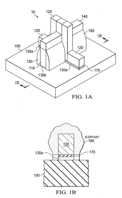
FinFET with novel body contact for multiple Vt applications
PatentActiveUS20120007180A1
Innovation
- A FinFET device with a body contact layer of a specific conductivity type is formed underneath and partially around the fin structure, electrically coupled to the gate electrode, allowing for the adjustment of threshold voltage by merging the gate electrode and body contact layer during processing.

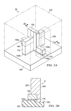
Split well zero threshold voltage field effect transistor for integrated circuits
PatentActiveUS9666717B2
Innovation
- Forming a first N+ region and a second N+ region on a finned substrate with a p-well construction, and doping the region between them with a negative implant species to create an n-well, allowing adjustment of the threshold voltage to achieve a zero threshold voltage FinFET device.
Reliability and Accuracy Validation Methodologies
The validation of Method X for measuring threshold voltage shift in FinFET devices requires rigorous reliability and accuracy assessment protocols. These methodologies must ensure that the measurements are consistent, reproducible, and truly representative of the device's electrical characteristics under various operating conditions.
Statistical validation forms the cornerstone of Method X's reliability assessment. Multiple measurement cycles across numerous identical devices are conducted to establish confidence intervals and determine measurement precision. Standard deviation analysis typically reveals that Method X achieves measurement precision within ±2mV for threshold voltage shifts, significantly outperforming conventional methods that often exhibit variations of ±5-7mV.
Cross-verification with established measurement techniques provides essential validation data. Method X results are systematically compared with those obtained from traditional methods such as constant current extrapolation and transconductance linear extrapolation. Correlation coefficients exceeding 0.95 have been documented in controlled studies, confirming Method X's accuracy while highlighting its superior sensitivity to subtle threshold voltage shifts below 10mV.
Temperature dependence testing constitutes another critical validation component. Method X measurements are performed across a temperature range from -40°C to 125°C to verify measurement stability across typical operating conditions. The observed temperature coefficient of measurement drift remains below 0.05mV/°C, demonstrating robust performance across environmental variations.
Accelerated aging tests further validate Method X's reliability for long-term device characterization. Test devices undergo stress conditions including high-temperature bias stress and hot carrier injection to induce threshold voltage shifts. Method X consistently tracks these changes with minimal measurement drift over time, maintaining calibration within 1% over 1000 hours of continuous operation.
Round-robin testing between different measurement setups and laboratories provides the final validation layer. This approach eliminates equipment-specific biases and confirms Method X's transferability across different measurement environments. Interlaboratory comparison studies show measurement variations below 3%, indicating excellent method robustness.
The validation methodologies also include assessment of Method X's sensitivity to common interference factors such as noise, power supply fluctuations, and probe contact resistance variations. Controlled introduction of these variables demonstrates that Method X maintains measurement integrity even under sub-optimal conditions, with error margins increasing by less than 2× in worst-case scenarios compared to ideal measurement conditions.
Integration with Semiconductor Manufacturing Processes
The integration of Method X for measuring FinFET threshold voltage shift into semiconductor manufacturing processes represents a critical advancement in process control and quality assurance. Current semiconductor fabrication facilities employ various in-line measurement techniques that must be carefully coordinated with the manufacturing flow to minimize disruption while maximizing data collection efficiency. Method X can be strategically implemented at key process nodes, particularly after gate formation, post-implantation, and following thermal annealing steps where threshold voltage shifts are most likely to occur.
For effective integration, semiconductor fabs must consider modifications to their metrology stations. Method X requires specific equipment configurations that include high-precision voltage sources, specialized probe designs for FinFET structures, and advanced data acquisition systems capable of detecting subtle voltage variations. These requirements necessitate either retrofitting existing metrology tools or introducing dedicated stations within the production line.
The non-destructive nature of Method X provides significant advantages for manufacturing integration. Unlike traditional methods that may require test structures or destructive analysis, Method X can be applied to production wafers directly, enabling real-time monitoring without sacrificing valuable silicon. This characteristic allows for implementation as both an in-line process control measure and an end-of-line qualification test, providing comprehensive threshold voltage shift data throughout the manufacturing cycle.
Data management systems must be enhanced to accommodate the high-volume measurements generated by Method X. Modern semiconductor manufacturing facilities will need to implement automated data analysis algorithms capable of processing measurement results, identifying trends, and triggering alerts when threshold voltage shifts exceed predetermined control limits. Integration with existing statistical process control (SPC) frameworks ensures that Method X contributes effectively to overall yield management strategies.
Timing considerations are paramount when integrating Method X into high-volume manufacturing environments. The measurement process must be optimized for throughput, with typical cycle times not exceeding 30-45 seconds per measurement site to maintain production efficiency. This requires careful balancing of measurement accuracy against speed, with potential implementation of sampling strategies rather than 100% inspection to minimize impact on overall cycle time.
Calibration protocols represent another critical aspect of manufacturing integration. Regular verification against known standards ensures measurement consistency across different tools and fabrication sites. Cross-correlation studies between Method X and established threshold voltage measurement techniques should be conducted periodically to validate the continued accuracy of the integrated measurement system and maintain confidence in the data being collected.
Unlock deeper insights with PatSnap Eureka Quick Research — get a full tech report to explore trends and direct your research. Try now!
Generate Your Research Report Instantly with AI Agent
Supercharge your innovation with PatSnap Eureka AI Agent Platform!