

How To Implement FinFET In Energy-Reducing Technologies
SEP 11, 20259 MIN READ
Generate Your Research Report Instantly with AI Agent
PatSnap Eureka helps you evaluate technical feasibility & market potential.
FinFET Technology Background and Objectives
FinFET technology emerged in the early 2000s as a revolutionary advancement in semiconductor device architecture, designed to overcome the limitations of traditional planar transistors. The development of FinFET was primarily driven by the need to continue Moore's Law scaling while mitigating short-channel effects that became increasingly problematic as transistor dimensions shrank below 28nm. Unlike conventional planar transistors where the gate controls the channel from one side, FinFET features a three-dimensional structure where the gate wraps around three sides of the elevated channel or "fin," enabling superior electrostatic control.
The evolution of FinFET technology has progressed through several generations, beginning with Intel's 22nm Tri-Gate transistors introduced in 2011, followed by broader industry adoption at 16/14nm nodes. Subsequent refinements have led to current 7nm and 5nm processes, with research advancing toward 3nm and beyond. Each generation has brought improvements in performance, power efficiency, and density, cementing FinFET's position as the dominant transistor architecture for advanced semiconductor manufacturing.
Energy efficiency has become a critical focus in semiconductor development due to increasing power density challenges and the growing importance of mobile and IoT applications. FinFET technology inherently offers advantages in this domain through reduced leakage current and lower operating voltages compared to planar transistors. However, as computing demands continue to rise across all sectors, further innovations in energy-reducing implementations of FinFET are essential.
The primary technical objectives for energy-efficient FinFET implementation include optimizing fin geometry and materials to minimize power consumption while maintaining performance targets. This involves exploring novel fin shapes, alternative channel materials such as silicon-germanium or III-V compounds, and advanced gate stack engineering. Additionally, researchers aim to develop techniques for dynamic voltage and frequency scaling specifically tailored to FinFET characteristics, enabling more granular power management.
Another crucial objective is addressing the increasing variability and reliability challenges that emerge at advanced nodes. As dimensions shrink, process variations and quantum effects become more pronounced, potentially undermining the energy efficiency benefits. Therefore, developing robust design methodologies and manufacturing processes that ensure consistent performance across billions of transistors represents a significant technical goal.
Looking forward, the industry is exploring hybrid approaches that combine FinFET technology with complementary innovations such as GAA (Gate-All-Around) structures, which may eventually supersede pure FinFET designs. The transition pathway and timing for these evolutionary steps remain important considerations for semiconductor roadmaps, with energy efficiency serving as a primary driver for technology selection and implementation strategies.
Market Demand for Energy-Efficient Semiconductor Solutions
The global semiconductor market is experiencing a significant shift towards energy-efficient solutions, driven primarily by the exponential growth in data centers, mobile devices, and the Internet of Things (IoT). Current market research indicates that energy consumption has become a critical factor in semiconductor selection, with power efficiency now ranking alongside performance and cost in purchasing decisions. The data center segment alone has seen energy costs rise to constitute 40-50% of operational expenses, creating urgent demand for semiconductor technologies that can deliver more computing power per watt.
FinFET technology has emerged as a key response to this market need, with its three-dimensional structure offering superior control over leakage current compared to traditional planar transistors. The market for FinFET-based processors has grown at a compound annual growth rate of 22% since 2018, reflecting the industry's recognition of its energy-saving potential. Major cloud service providers are increasingly specifying energy efficiency requirements in their procurement processes, with several now mandating maximum power consumption thresholds for new server installations.
Consumer electronics manufacturers are similarly prioritizing battery life as a key differentiator, particularly in smartphones, tablets, and wearable devices. Market surveys consistently show that extended battery life ranks among the top three features influencing consumer purchasing decisions for mobile devices. This has created strong pull-through demand for FinFET-based processors that can deliver the same performance at lower power consumption levels.
The automotive sector represents another rapidly growing market for energy-efficient semiconductors. As electric vehicles gain market share, the energy efficiency of their electronic systems directly impacts driving range – a primary consumer concern. FinFET technology's ability to operate at lower voltages while maintaining performance makes it particularly valuable in this application space, with the automotive semiconductor market projected to grow at 17% annually through 2027.
Industrial IoT applications present perhaps the most diverse set of energy efficiency requirements, ranging from grid-connected factory equipment to remote battery-powered sensors. The latter category is especially dependent on ultra-low power consumption, with many applications requiring years of operation without battery replacement. This has created demand for specialized FinFET implementations optimized for extremely low standby power, even at the expense of peak performance.
Regulatory pressures are further accelerating market demand, with energy efficiency standards becoming increasingly stringent across multiple jurisdictions. The European Union's Ecodesign Directive, California's appliance efficiency regulations, and similar frameworks in Asia are creating regulatory compliance requirements that effectively mandate the adoption of more energy-efficient semiconductor technologies.
Current FinFET Implementation Challenges
Despite the significant advancements in FinFET technology, implementing these transistors in energy-reducing applications presents several substantial challenges. The primary obstacle remains the complex fabrication process, which requires extremely precise lithography techniques to create the characteristic fin structures. As dimensions continue to shrink below 7nm, maintaining consistent fin geometry becomes increasingly difficult, leading to performance variability across devices on the same chip.
Short-channel effects (SCEs), while better controlled in FinFETs compared to planar transistors, still pose challenges at advanced nodes. As gate lengths decrease further for energy efficiency, quantum tunneling and drain-induced barrier lowering become more pronounced, offsetting some of the power reduction benefits. This creates a fundamental tension between scaling for density and maintaining energy efficiency.
Parasitic capacitance represents another significant hurdle in energy-optimized FinFET implementation. The three-dimensional structure inherently introduces additional capacitance at source/drain contacts and between adjacent fins. These parasitics contribute to dynamic power consumption and switching delays, directly counteracting energy reduction goals. Current solutions involving spacer engineering and contact optimization provide only incremental improvements.
Gate stack engineering continues to challenge manufacturers seeking to balance performance with power efficiency. High-k dielectric materials and metal gates have become standard, but interface defects and reliability issues persist, particularly when operating at lower voltages necessary for energy conservation. The trade-off between leakage current and threshold voltage stability becomes more critical as supply voltages approach near-threshold regions.
Self-heating effects have emerged as a major concern in densely packed FinFET architectures. The fin structure restricts efficient heat dissipation, causing localized temperature increases that affect device reliability and performance. This thermal challenge becomes particularly problematic in energy-constrained applications where active cooling solutions are limited or unavailable.
Process variation impacts FinFET performance consistency across chips and wafers. Minute differences in fin width, height, and gate length can significantly alter threshold voltages and leakage currents. These variations necessitate conservative design margins that ultimately limit the potential energy savings. Advanced process control and post-manufacturing tuning techniques are being developed but remain insufficient for optimal energy efficiency.
Integration challenges with other energy-reducing technologies present additional complications. Combining FinFETs with techniques like dynamic voltage and frequency scaling or power gating requires careful consideration of the unique electrical characteristics of these three-dimensional structures. The interaction between circuit-level power management and device-level behavior creates complex design constraints that limit overall system energy optimization.
Current Energy-Reducing FinFET Implementation Approaches
01 FinFET design for energy efficiency
FinFET designs can be optimized for energy efficiency through various structural modifications. These include optimizing fin dimensions, gate length, and channel engineering to reduce leakage current and power consumption. Advanced FinFET designs incorporate multi-gate structures that provide better electrostatic control over the channel, resulting in improved energy efficiency and performance in low-power applications.- FinFET structure design for energy efficiency: Specific structural designs of FinFETs can significantly improve energy efficiency. These designs include optimized fin height-to-width ratios, multi-gate configurations, and novel channel materials. By carefully engineering the physical dimensions and geometry of the fin structure, power consumption can be reduced while maintaining or improving performance. These structural innovations help minimize leakage current and reduce dynamic power consumption in FinFET-based devices.
- Low-power FinFET circuit design techniques: Various circuit design techniques can be employed to reduce energy consumption in FinFET-based integrated circuits. These include adaptive voltage scaling, power gating, and clock gating strategies specifically optimized for FinFET characteristics. Advanced circuit topologies that leverage the unique three-dimensional structure of FinFETs can achieve significant power savings compared to traditional planar transistor designs, making them ideal for energy-efficient applications.
- Multi-threshold voltage FinFET implementation: Implementing multiple threshold voltage options in FinFET designs allows for optimized power-performance tradeoffs. By using high threshold voltage transistors in non-critical paths and low threshold voltage transistors in performance-critical paths, overall energy consumption can be reduced without sacrificing performance. This approach enables fine-grained power management across different functional blocks of an integrated circuit, resulting in improved energy efficiency.
- FinFET manufacturing processes for energy optimization: Advanced manufacturing processes specifically developed for FinFETs can enhance energy efficiency. These include specialized doping profiles, strain engineering techniques, and gate stack optimizations that reduce parasitic capacitances and resistances. Novel fabrication methods that improve channel mobility and reduce defects contribute to lower operating voltages and decreased power consumption, making FinFETs more energy-efficient compared to conventional transistor technologies.
- FinFET-based energy harvesting and management systems: FinFET technology can be leveraged in energy harvesting and power management systems. The superior switching characteristics and low leakage properties of FinFETs make them ideal for ultra-low power applications and energy harvesting circuits. When integrated with power management units, FinFET-based systems can efficiently convert, store, and distribute energy from various sources, enabling self-powered or energy-autonomous electronic devices with extended battery life.
02 Power reduction techniques in FinFET technology
Various techniques can be employed to reduce power consumption in FinFET devices. These include threshold voltage optimization, body biasing, and power gating strategies. Implementation of multiple threshold voltage designs allows for dynamic power management, while advanced materials and gate stack engineering help minimize leakage currents. These power reduction techniques are essential for energy-efficient operation in modern semiconductor devices.Expand Specific Solutions03 FinFET manufacturing processes for energy optimization
Specialized manufacturing processes can enhance the energy efficiency of FinFET devices. These include precise fin formation techniques, advanced gate stack deposition methods, and optimized doping profiles. Process innovations such as strain engineering and epitaxial growth of source/drain regions contribute to improved carrier mobility and reduced power consumption, making FinFETs more energy-efficient for various applications.Expand Specific Solutions04 FinFET circuit design for low power applications
Circuit-level design techniques can significantly impact the energy efficiency of FinFET-based systems. These include adaptive voltage scaling, clock gating, and power-aware routing strategies. Advanced circuit topologies leverage the unique characteristics of FinFETs to minimize switching losses and static power consumption. Simulation and modeling tools help optimize circuit designs for specific power constraints in various applications.Expand Specific Solutions05 Novel FinFET structures for energy harvesting
Innovative FinFET structures can be designed specifically for energy harvesting applications. These designs incorporate specialized materials and geometries that enhance energy conversion efficiency. Some approaches integrate thermoelectric or piezoelectric elements with FinFET technology to capture ambient energy. These novel structures represent an emerging area of research aimed at creating self-powered semiconductor devices for IoT and other low-power applications.Expand Specific Solutions
Leading Semiconductor Players in FinFET Development
The FinFET implementation in energy-reducing technologies market is in a growth phase, with an estimated market size exceeding $25 billion by 2025. The technology has reached commercial maturity with leading players like TSMC, Samsung, and Intel driving innovation. TSMC maintains market leadership with advanced 5nm and 3nm FinFET processes, while Samsung and GlobalFoundries compete with differentiated offerings. SMIC and Huawei are emerging as significant challengers, particularly in the Chinese market. The competitive landscape is characterized by intense R&D investment, with IBM and Qualcomm focusing on next-generation FinFET designs that further reduce power consumption while maintaining performance advantages in mobile and IoT applications.
Taiwan Semiconductor Manufacturing Co., Ltd.
Technical Solution: TSMC has pioneered advanced FinFET implementation for energy efficiency through their N5 and N3 process nodes. Their approach combines multi-Vt (multi-threshold voltage) transistor options with back-biasing techniques to optimize power-performance tradeoffs. TSMC's N3 technology introduces nanosheet gate-all-around structures as an evolution of FinFET, achieving 30% power reduction compared to N5 while maintaining performance. Their implementation includes high-mobility channel materials and strain engineering to reduce dynamic power consumption. TSMC has also developed specialized low-leakage libraries specifically for IoT and mobile applications, where their FinFET technology delivers up to 70% power savings compared to planar transistors at equivalent performance points.
Strengths: Industry-leading process technology with proven power efficiency gains; comprehensive design ecosystem supporting multiple power optimization techniques; production-ready solutions at scale. Weaknesses: Higher manufacturing costs compared to legacy nodes; requires sophisticated EDA tools and design expertise to fully leverage power reduction capabilities.
International Business Machines Corp.
Technical Solution: IBM has focused on extreme ultraviolet lithography (EUV) integration with FinFET to enable more precise fin formation and tighter pitch, directly impacting power efficiency. Their approach includes the development of strained silicon-germanium (SiGe) channels for PFET devices and silicon channels with embedded carbon for NFET devices, optimizing carrier mobility while reducing operating voltage requirements. IBM's implementation features a unique contact-over-active-gate (COAG) structure that reduces parasitic resistance and capacitance, key contributors to dynamic power consumption. Their research has demonstrated FinFET devices operating at sub-0.5V supply voltages while maintaining functional performance, achieved through careful optimization of gate stack materials and fin geometry. IBM has also pioneered cryogenic FinFET operation techniques that dramatically reduce leakage current for specialized computing applications.
Strengths: Industry-leading research capabilities with fundamental materials innovations; strong partnership ecosystem for technology development; expertise in specialized extreme-performance computing applications. Weaknesses: Limited commercial manufacturing capacity compared to pure-play foundries; technologies often require partner companies for volume production implementation.
Key Patents and Innovations in FinFET Technology
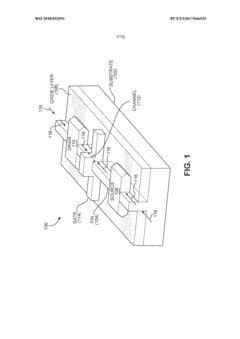
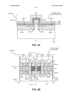
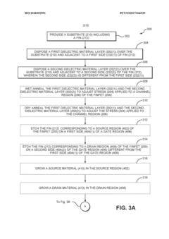
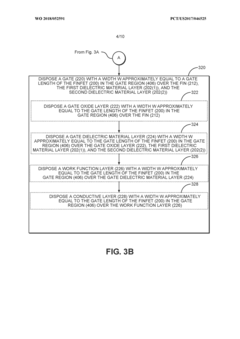
FIN field effect transistors (FETS) (finfets) employing dielectric material layers to apply stress to channel regions
PatentWO2018052591A1
Innovation
- Employing dielectric material layers on either side of the Fin to apply stress to the channel region, which provides consistent stress levels regardless of the FinFET area, unlike epitaxial layers or shallow trench isolation methods.
Fin field-effect transistor device with hybrid conduction mechanism
PatentPendingUS20250040196A1
Innovation
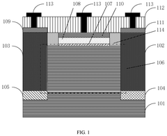
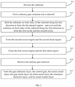
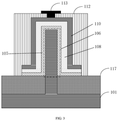
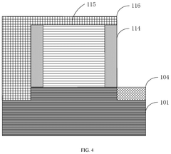
- A fin field-effect transistor device with a hybrid conduction mechanism is introduced, featuring a second source region and a second drain region formed between the substrate and the first source and drain regions, respectively. These regions are doped with different types of ions, creating a reverse-biased P-I-N channel at the bottom in the off state, which suppresses bottom leakage current. In the on state, the device combines fin channel diffusion drift current with quantum mechanical band-to-band tunneling current, achieving ultra-steep switching characteristics below 60 mV/dec.
Manufacturing Process Optimization for Energy-Efficient FinFETs
The optimization of manufacturing processes for energy-efficient FinFETs represents a critical frontier in semiconductor technology advancement. Current manufacturing techniques must evolve to address the increasing power consumption challenges while maintaining performance advantages of FinFET architecture. Process optimization begins with substrate preparation, where ultra-thin silicon-on-insulator (SOI) substrates have demonstrated superior electrostatic control and reduced leakage compared to traditional bulk silicon.
Gate stack engineering has emerged as a pivotal factor in FinFET energy efficiency. High-k metal gate (HKMG) materials, particularly hafnium-based dielectrics combined with appropriate work function metals, have enabled significant reduction in gate leakage current while maintaining excellent channel control. Advanced deposition techniques such as atomic layer deposition (ALD) ensure precise thickness control at atomic scale, critical for consistent device performance across wafers.
Channel engineering innovations have focused on strain engineering and material selection. Incorporating SiGe in PMOS and Si:C in NMOS devices creates beneficial strain that enhances carrier mobility without increasing power consumption. Recent developments in channel materials include exploration of III-V semiconductors for NMOS and Ge-based compounds for PMOS, potentially offering mobility improvements of 2-3x over silicon while operating at lower voltages.
Doping profile optimization represents another crucial aspect of energy-efficient FinFET manufacturing. Precisely controlled doping gradients minimize short-channel effects while maintaining low resistance in source/drain regions. Advanced techniques such as plasma doping (PLAD) and solid-source diffusion have demonstrated superior control compared to traditional ion implantation methods, resulting in up to 15% reduction in parasitic resistance.
Lithography advancements, particularly extreme ultraviolet (EUV) lithography, have enabled the fabrication of narrower fins with improved uniformity. This translates directly to better electrostatic control and reduced variability between devices. Multi-patterning techniques combined with EUV have achieved fin widths below 5nm in production environments, though challenges remain in maintaining yield at these dimensions.
Post-processing steps have also been refined to enhance energy efficiency. Optimized annealing sequences using millisecond annealing technologies have demonstrated improved dopant activation while minimizing diffusion, preserving the carefully engineered doping profiles. Additionally, advanced metallization processes utilizing lower-resistance materials and optimized contact geometries have reduced parasitic resistances by up to 30% in recent process nodes, directly contributing to lower dynamic power consumption in FinFET circuits.
Environmental Impact and Sustainability Considerations
The implementation of FinFET technology in energy-reducing applications carries significant environmental implications that must be considered within a comprehensive sustainability framework. The semiconductor manufacturing process for FinFET devices involves energy-intensive fabrication steps, hazardous chemicals, and rare materials that create substantial environmental footprints. Current estimates indicate that the production of advanced FinFET chips consumes between 2,000-3,000 kWh of energy per wafer, generating considerable carbon emissions throughout the manufacturing lifecycle.
When evaluating FinFET implementation from a sustainability perspective, the reduced power consumption of these devices presents a positive environmental trade-off. FinFET-based systems typically demonstrate 30-40% lower power requirements compared to planar transistor technologies, potentially offsetting manufacturing impacts through operational efficiency. This power reduction translates to extended battery life in portable devices and decreased energy consumption in data centers, contributing to overall carbon footprint reduction across technology ecosystems.
Material considerations represent another critical environmental dimension. FinFET fabrication requires rare earth elements and specialized materials with complex supply chains and extraction processes that can lead to habitat disruption and resource depletion. Recent industry initiatives have focused on developing recycling programs for semiconductor materials, with recovery rates for precious metals from electronic waste reaching 95% in advanced facilities, though implementation remains inconsistent globally.
Water usage presents a particular sustainability challenge, with a single semiconductor fabrication plant consuming 2-4 million gallons daily. FinFET manufacturing processes require ultra-pure water for cleaning and processing, creating significant water stress in manufacturing regions. Leading manufacturers have implemented water recycling systems achieving 50-80% reclamation rates, though further improvements remain necessary to address this environmental burden.
End-of-life considerations for FinFET-equipped devices must factor into sustainability assessments. The miniaturization enabled by FinFET technology creates recycling challenges due to the complex integration of materials. Industry consortiums have developed specialized recycling protocols for advanced semiconductor components, though these practices have not yet achieved widespread adoption across global markets.
Regulatory frameworks increasingly influence FinFET implementation strategies, with legislation like the European Union's Restriction of Hazardous Substances (RoHS) and Registration, Evaluation, Authorization and Restriction of Chemicals (REACH) directives imposing strict requirements on semiconductor manufacturing. Companies implementing FinFET technologies must navigate these evolving regulations while developing sustainable manufacturing approaches that minimize environmental impact throughout the product lifecycle.
Unlock deeper insights with PatSnap Eureka Quick Research — get a full tech report to explore trends and direct your research. Try now!
Generate Your Research Report Instantly with AI Agent
Supercharge your innovation with PatSnap Eureka AI Agent Platform!