

Stimulating FinFET Processing: Impacts On Efficiency
SEP 11, 20259 MIN READ
Generate Your Research Report Instantly with AI Agent
PatSnap Eureka helps you evaluate technical feasibility & market potential.
FinFET Technology Background and Objectives
FinFET (Fin Field-Effect Transistor) technology emerged as a revolutionary advancement in semiconductor manufacturing, addressing the scaling limitations of traditional planar transistors. Developed in the early 2000s, FinFETs represent a three-dimensional transistor architecture where the gate wraps around a thin silicon "fin" that forms the transistor channel. This design significantly reduces leakage current and enables better electrostatic control of the channel, allowing for continued miniaturization according to Moore's Law.
The evolution of FinFET technology has progressed through several generations, from 22nm to the current advanced nodes at 5nm and below. Each generation has brought improvements in performance, power efficiency, and transistor density. The technology has become the backbone of modern high-performance computing, mobile devices, and data centers, enabling unprecedented computational capabilities while managing power consumption.
Current technological trends in FinFET development focus on overcoming quantum effects and physical limitations as dimensions approach atomic scales. Research directions include novel materials integration, advanced lithography techniques, and innovative device architectures to extend FinFET scalability. Additionally, there is significant interest in enhancing manufacturing processes to improve yield and reduce variability, which becomes increasingly challenging at smaller nodes.
The primary objectives of FinFET technology research center on maximizing efficiency across multiple dimensions. Performance efficiency aims to increase transistor switching speed while maintaining reliability. Power efficiency focuses on reducing dynamic and static power consumption, critical for battery-powered devices and data centers. Area efficiency targets higher transistor density to enable more functionality per unit area. Manufacturing efficiency seeks to optimize production processes, reducing costs and environmental impact.
Stimulating FinFET processing specifically addresses the challenges in manufacturing these complex three-dimensional structures with atomic precision. This involves innovations in deposition, etching, and annealing processes to form perfect fin structures with minimal defects. Advanced simulation tools have become essential for predicting and optimizing these processes before physical implementation, reducing development cycles and costs.
The ultimate goal of current FinFET technology development is to push the boundaries of what's physically possible in semiconductor manufacturing while maintaining economic viability. This includes exploring hybrid approaches that combine FinFET advantages with emerging technologies like gate-all-around structures, which may eventually succeed FinFETs in the semiconductor roadmap. Understanding these technological trajectories is crucial for strategic planning in the semiconductor industry.
Market Demand Analysis for Advanced Semiconductor Nodes
The semiconductor industry has witnessed a significant shift in market demand towards advanced nodes, particularly those utilizing FinFET technology. Current market analysis indicates that the global semiconductor industry is valued at approximately $550 billion, with advanced nodes representing over 40% of this market. The transition from planar transistors to FinFET architecture has been driven by the increasing demand for higher performance, lower power consumption, and smaller form factors in electronic devices.
Consumer electronics, particularly smartphones and tablets, constitute the largest market segment for advanced semiconductor nodes, accounting for roughly 35% of total demand. The continuous push for more powerful yet energy-efficient mobile devices has accelerated the adoption of FinFET technology across multiple generations, from 22nm down to current 5nm and 3nm nodes.
Data centers and cloud computing infrastructure represent the fastest-growing segment, with an annual growth rate of 25%. This surge is attributed to the exponential increase in data processing requirements, artificial intelligence applications, and the overall digital transformation across industries. Advanced FinFET nodes are critical in meeting the computational demands while managing power consumption in these high-performance computing environments.
Automotive electronics has emerged as a promising market for advanced semiconductor nodes, particularly with the rise of electric vehicles and autonomous driving technologies. The automotive sector's semiconductor content is growing at 15% annually, with advanced nodes increasingly being adopted for critical systems requiring high reliability and performance under varying environmental conditions.
Geographic distribution of demand shows Asia-Pacific leading with 60% of the market, primarily driven by manufacturing hubs in Taiwan, South Korea, and increasingly China. North America follows with 20%, largely due to data center expansion and high-end computing applications. Europe accounts for 15%, with strength in automotive and industrial applications.
Market forecasts indicate that demand for advanced nodes will continue to grow at a compound annual rate of 8% over the next five years. However, this growth is accompanied by increasing challenges in manufacturing economics. The cost per transistor, which historically decreased with each node advancement, has begun to plateau or even increase at the most advanced nodes, creating a complex value proposition for semiconductor manufacturers and their customers.
The efficiency improvements offered by FinFET processing technologies remain a critical factor in market adoption decisions, with customers increasingly evaluating the performance-per-watt metrics rather than raw performance alone. This shift has significant implications for how semiconductor companies position their advanced node offerings and the research priorities they establish for future technology development.
Current FinFET Processing Challenges and Limitations
Despite significant advancements in FinFET technology over the past decade, current processing methodologies face several critical challenges that limit manufacturing efficiency and device performance. The primary limitation stems from the increasing complexity of three-dimensional fin structures as node sizes continue to shrink below 7nm. This complexity introduces significant variability in fin height, width, and profile, directly impacting transistor performance characteristics and yield rates.
Material deposition uniformity presents another substantial challenge, particularly for high-aspect-ratio structures. Current atomic layer deposition (ALD) and chemical vapor deposition (CVD) techniques struggle to achieve consistent coverage on vertical fin sidewalls, creating potential weak points in the gate dielectric and subsequent reliability issues. These non-uniformities become increasingly problematic as fin dimensions approach sub-5nm widths.
Etching processes face precision limitations that directly affect FinFET efficiency. The industry currently struggles with achieving the perfect balance between anisotropic etching for vertical fin profiles and minimizing damage to the silicon crystal structure. Plasma-induced damage during dry etching processes can degrade carrier mobility and increase leakage current, compromising the power efficiency advantages that FinFETs theoretically offer.
Doping challenges represent another significant limitation in current processing techniques. As fins become narrower, conventional ion implantation methods create excessive crystal damage and struggle to achieve uniform dopant distribution throughout the three-dimensional structure. This non-uniformity leads to variability in threshold voltages and suboptimal device performance.
Metrology and inspection capabilities have not kept pace with manufacturing requirements. Current in-line measurement techniques lack the precision needed to accurately characterize fin dimensions and defects at advanced nodes, creating a significant blind spot in process control. This limitation forces manufacturers to rely on indirect measurements and statistical process control rather than direct observation of critical features.
Integration challenges with middle-of-line and back-end-of-line processes further complicate FinFET manufacturing. Contact formation to the raised source/drain regions requires extremely precise alignment and etching capabilities that push the limits of current lithography systems. Additionally, the high-aspect-ratio contacts needed for FinFET structures create resistance and reliability concerns that impact overall circuit performance.
Thermal budget constraints have become increasingly restrictive with each technology node. The need to maintain fin integrity while performing necessary high-temperature steps for dopant activation and silicidation creates fundamental trade-offs between structural stability and electrical performance. These thermal limitations restrict process options and potentially compromise device characteristics.
Current Stimulation Techniques in FinFET Manufacturing
01 FinFET structure optimization
Optimizing the structure of FinFETs can significantly improve processing efficiency. This includes modifications to the fin shape, height, and width to enhance performance characteristics. Advanced fin designs with optimized dimensions can reduce parasitic capacitance and improve current flow. These structural optimizations contribute to better electrical characteristics and overall device efficiency while maintaining manufacturability.- Advanced FinFET fabrication techniques: Various fabrication techniques have been developed to improve FinFET processing efficiency. These include optimized fin formation processes, selective epitaxial growth methods, and precise etching techniques that enhance device performance while reducing manufacturing complexity. These advanced techniques allow for better control of fin dimensions and profiles, resulting in improved electrical characteristics and higher yield rates.
- Multi-gate transistor design optimization: Optimizing the design of multi-gate transistors, particularly FinFETs, can significantly improve processing efficiency. This includes innovations in gate structure, channel engineering, and source/drain formation. By carefully designing these elements, manufacturers can achieve better performance characteristics while simplifying the fabrication process, leading to higher throughput and reduced production costs.
- Integration of FinFETs with complementary technologies: Efficient integration of FinFET technology with other semiconductor technologies enhances overall processing efficiency. This includes methods for combining FinFETs with conventional planar transistors, memory elements, or other circuit components. Such integration techniques reduce the number of processing steps, improve compatibility between different device types, and enable more efficient manufacturing workflows.
- Computational methods for FinFET design and manufacturing: Advanced computational methods and simulation tools have been developed to optimize FinFET design and manufacturing processes. These include automated layout generation, process simulation, and design verification techniques that help identify potential issues before physical fabrication. By leveraging these computational approaches, manufacturers can reduce design iterations, optimize process parameters, and improve overall production efficiency.
- Novel materials and structures for enhanced FinFET performance: The introduction of novel materials and structural innovations can significantly improve FinFET processing efficiency. These include high-mobility channel materials, advanced gate dielectrics, and innovative contact structures that enhance device performance while potentially simplifying the manufacturing process. By incorporating these materials and structural designs, manufacturers can achieve better electrical characteristics with fewer processing steps.
02 Multi-gate transistor fabrication techniques
Novel fabrication techniques for multi-gate transistors, including FinFETs, can enhance processing efficiency. These techniques involve innovative approaches to gate formation, channel engineering, and source/drain formation. By implementing advanced fabrication methods, manufacturers can achieve better control over critical dimensions, reduce process variations, and improve yield. These techniques often focus on simplifying the manufacturing process while maintaining or improving device performance.Expand Specific Solutions03 Design automation and simulation for FinFET processing
Computer-aided design tools and simulation techniques specifically developed for FinFET processing can significantly improve efficiency. These tools enable accurate modeling of complex three-dimensional structures, prediction of electrical characteristics, and optimization of process parameters. By utilizing advanced design automation and simulation, manufacturers can reduce development cycles, minimize experimental iterations, and achieve faster time-to-market for FinFET-based products.Expand Specific Solutions04 Integration of novel materials in FinFET processing
Incorporating novel materials into FinFET fabrication can enhance processing efficiency and device performance. These materials include high-k dielectrics, metal gates, strain-inducing materials, and advanced contact metals. The integration of these materials requires specialized processing techniques but can result in significant improvements in transistor performance, power consumption, and reliability. Careful selection and optimization of materials can address challenges related to scaling and performance limitations.Expand Specific Solutions05 Advanced etching and patterning techniques for FinFETs
Specialized etching and patterning techniques are crucial for efficient FinFET processing. These include advanced lithography methods, self-aligned double patterning, sidewall image transfer, and precise fin definition processes. By implementing these techniques, manufacturers can achieve better control over fin dimensions, reduce variability, and improve yield. These advanced processes enable the fabrication of high-density, high-performance FinFET devices with enhanced efficiency and reliability.Expand Specific Solutions
Key Semiconductor Industry Players and Competition
The FinFET processing technology market is currently in a mature growth phase, with an estimated global market size exceeding $50 billion and projected to expand at a CAGR of 12-15% through 2028. The competitive landscape is dominated by established players like TSMC, Samsung, and GlobalFoundries, who lead in efficiency optimization through advanced node development. TSMC maintains technological superiority with its 3nm FinFET process, while Samsung and Intel are aggressively investing in GAA-FET transitions. Chinese manufacturers including SMIC are rapidly advancing despite restrictions, focusing on specialized applications. Qualcomm and Micron represent the customer segment driving innovation demands. The technology has reached commercial maturity but continues evolving toward more efficient architectures as traditional FinFET approaches physical scaling limitations.
Taiwan Semiconductor Manufacturing Co., Ltd.
Technical Solution: TSMC has pioneered advanced FinFET processing technologies with their leading-edge nodes (7nm, 5nm, and 3nm). Their approach involves multi-patterning techniques and advanced lithography to create high-aspect-ratio fins with precise control. TSMC employs strain engineering methods including SiGe source/drain regions and metal gate stress to enhance carrier mobility. Their FinFET process incorporates high-k metal gate (HKMG) technology with carefully selected work function metals to optimize threshold voltages. TSMC has also developed specialized doping profiles and junction engineering to minimize leakage currents while maintaining high drive currents. Their manufacturing process includes self-aligned contacts and advanced metallization schemes to reduce parasitic resistances and capacitances, significantly improving overall device performance and efficiency.
Strengths: Industry-leading process technology with highest transistor density and performance; excellent power efficiency characteristics; mature manufacturing ecosystem with high yields. Weaknesses: Higher manufacturing costs compared to planar technologies; complex process integration requiring sophisticated equipment and expertise.
QUALCOMM, Inc.
Technical Solution: As a fabless semiconductor company, Qualcomm has developed extensive expertise in FinFET design optimization while working closely with manufacturing partners like TSMC and Samsung. Their approach focuses on architectural innovations that maximize the benefits of FinFET technology for mobile and edge computing applications. Qualcomm employs advanced multi-threshold voltage design techniques to optimize power-performance tradeoffs in their SoCs. Their designs incorporate sophisticated power gating and dynamic voltage/frequency scaling specifically optimized for FinFET characteristics. Qualcomm has developed specialized circuit design methodologies to address FinFET-specific challenges like increased variability and self-heating effects. Their approach includes custom standard cell libraries optimized for FinFET processes with careful consideration of layout-dependent effects. Qualcomm's designs leverage FinFET advantages through architectural partitioning that places high-performance blocks in optimal process variants while using power-optimized options for less critical functions.
Strengths: Industry-leading expertise in FinFET design optimization for mobile applications; sophisticated power management techniques; strong relationships with multiple foundry partners. Weaknesses: Dependent on foundry partners for manufacturing technology advancement; limited control over fundamental process development; exposure to foundry capacity constraints.
Core Patents and Innovations in FinFET Stimulation
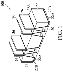
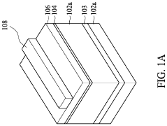
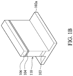
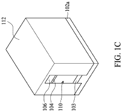
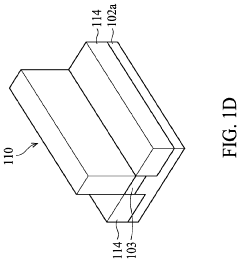
Reduction of Fin Loss in the Formation of FinFETs
PatentActiveUS20200295163A1
Innovation
- A method involving the formation of a gate spacer layer with selective implantation of ionic species at tilted angles to minimize damage to semiconductor fins, followed by a thermal anneal to repair and re-crystallize the damaged regions, and subsequent etching to remove the implanted portions of the gate spacer layer, thereby reducing fin loss and enhancing FinFET performance.
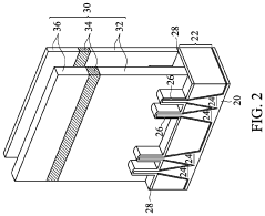
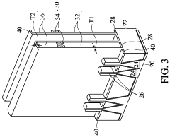
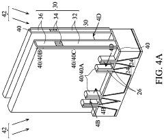
Fin field effect transistor (finfet) device structure with stop layer and method for forming the same
PatentActiveUS20210050447A1
Innovation
- Incorporating a stop layer with a different lattice constant than the substrate and gate materials, which serves as an etching stop and helps control the etching profile, allowing for precise formation of the fin structure and reducing the loading effect, thereby enhancing the etching uniformity and device performance.
Environmental Impact of FinFET Processing Technologies
The environmental footprint of FinFET processing technologies represents a critical consideration in semiconductor manufacturing sustainability. As these advanced transistor architectures continue to dominate high-performance computing applications, their production processes generate significant environmental impacts that warrant comprehensive assessment and mitigation strategies.
FinFET fabrication requires substantial energy consumption, primarily due to the complex multi-step lithography processes and high-temperature operations. Current estimates indicate that a typical semiconductor fabrication facility utilizing FinFET technology consumes between 30-50 MW of power continuously, equivalent to the energy needs of approximately 30,000 households. This intensive energy demand contributes significantly to carbon emissions, particularly in regions where electricity generation relies heavily on fossil fuels.
Water usage presents another major environmental concern in FinFET processing. The manufacturing process requires ultra-pure water for cleaning and rinsing operations, with a single fabrication facility consuming between 2-4 million gallons daily. This substantial water footprint becomes particularly problematic in water-stressed regions, creating potential conflicts with community needs and raising questions about long-term sustainability.
Chemical utilization in FinFET processing introduces additional environmental challenges. The fabrication process employs numerous hazardous substances including hydrofluoric acid, sulfuric acid, and various heavy metals. These chemicals require specialized handling, treatment, and disposal protocols to prevent environmental contamination. Recent industry data suggests that a typical semiconductor facility generates approximately 5,000-7,000 metric tons of chemical waste annually, necessitating sophisticated waste management systems.
Greenhouse gas emissions represent a growing concern in FinFET manufacturing. The process utilizes perfluorocarbons (PFCs) and other high global warming potential gases for plasma etching and chamber cleaning. These compounds can persist in the atmosphere for thousands of years and possess global warming potentials thousands of times greater than carbon dioxide. Industry estimates indicate that semiconductor manufacturing contributes approximately 0.2% of global greenhouse gas emissions.
Leading semiconductor manufacturers have begun implementing sustainability initiatives to address these environmental impacts. These include transitioning to renewable energy sources, implementing closed-loop water recycling systems, and developing alternative processing chemicals with reduced environmental persistence. Taiwan Semiconductor Manufacturing Company (TSMC), for instance, has committed to 100% renewable energy usage by 2050 and has already achieved 92% water recycling rates at some facilities.
Supply Chain Considerations for Advanced Node Manufacturing
The advanced manufacturing of FinFET devices at sub-7nm nodes presents significant supply chain challenges that directly impact production efficiency and economic viability. Semiconductor fabrication at these advanced nodes requires an increasingly complex and globally distributed supply chain network. Key materials such as high-purity silicon wafers, specialized chemicals, and rare gases face frequent supply constraints, with some critical components sourced from limited geographical regions. This concentration creates vulnerability to geopolitical tensions, natural disasters, and other disruptions as evidenced by recent global semiconductor shortages.
Equipment procurement represents another critical supply chain consideration, with lithography systems, etching tools, and metrology equipment often having lead times exceeding 12-18 months. The extreme precision required for FinFET processing has created a bottleneck where only a handful of suppliers can provide the necessary equipment, leading to dependency risks and potential production delays when demand surges.
Intellectual property management across the supply chain introduces additional complexity. Advanced node manufacturing involves hundreds of patented processes, with licensing agreements and technology transfer protocols requiring careful navigation. Companies must balance proprietary technology protection with the need for collaboration across the ecosystem to enable innovation in FinFET processing techniques.
Workforce considerations present another dimension of supply chain management. The specialized engineering talent required for advanced node manufacturing is scarce globally, with significant competition for experienced professionals in process integration, yield management, and equipment maintenance. Companies must develop robust talent pipelines and knowledge transfer mechanisms to maintain operational continuity.
Quality control across the extended supply chain is paramount for FinFET manufacturing efficiency. Contamination at parts-per-trillion levels can significantly impact device performance, necessitating stringent supplier qualification processes and real-time monitoring systems throughout the supply network. Advanced analytics and traceability systems have become essential for maintaining quality standards across geographically dispersed operations.
Inventory management strategies must evolve to balance the high capital costs of stockpiling expensive materials against the risk of production interruptions. Just-in-time approaches that worked for less advanced nodes prove inadequate for FinFET manufacturing, where certain specialized materials have limited shelf life and strict storage requirements. Companies are increasingly adopting hybrid inventory models with strategic buffers for critical components.
Unlock deeper insights with PatSnap Eureka Quick Research — get a full tech report to explore trends and direct your research. Try now!
Generate Your Research Report Instantly with AI Agent
Supercharge your innovation with PatSnap Eureka AI Agent Platform!