

FinFET Strain Effects On Device Performance: Quantitative Evaluation
SEP 11, 20259 MIN READ
Generate Your Research Report Instantly with AI Agent
PatSnap Eureka helps you evaluate technical feasibility & market potential.
FinFET Strain Technology Evolution and Objectives
The evolution of FinFET technology represents a pivotal advancement in semiconductor manufacturing, with strain engineering emerging as a critical factor in enhancing device performance. Since the introduction of commercial FinFET devices in 2011, strain effects have been systematically incorporated to overcome the limitations of conventional planar transistors. The initial generations of FinFET devices utilized intrinsic strain from SiGe source/drain regions, achieving modest performance improvements of 10-15% in carrier mobility.
As process nodes advanced from 22nm to 16/14nm, manufacturers implemented more sophisticated strain techniques, including dual stress liners and embedded SiGe/SiC, resulting in performance gains of approximately 25-30%. The evolution continued with the 10nm and 7nm nodes, where strain engineering became increasingly complex with the integration of channel materials featuring inherent strain properties and the development of strain retention techniques during the fin formation process.
The primary objective of strain engineering in FinFET devices is to enhance carrier mobility without compromising electrostatic control. Specifically, compressive strain aims to improve hole mobility in p-type FinFETs, while tensile strain targets electron mobility enhancement in n-type devices. Quantitative evaluations indicate that properly engineered strain can improve drive current by up to 45% in advanced nodes, directly impacting switching speeds and power efficiency.
Another critical objective is maintaining strain uniformity throughout the three-dimensional fin structure. Early FinFET generations struggled with strain relaxation at fin edges and corners, leading to performance variability. Recent technological advancements have focused on developing strain distribution models and fabrication techniques that ensure consistent strain profiles across the entire channel region, with variations now limited to less than 5% in leading-edge processes.
Looking forward, the industry aims to achieve precise strain control at atomic scales, particularly as fin dimensions continue to shrink below 5nm. Research indicates that strain engineering will remain essential even as the industry transitions to gate-all-around (GAA) and nanosheet architectures, with simulation models predicting potential performance improvements of 50-60% through next-generation strain techniques such as heteroepitaxial growth of channel materials and strain-engineered gate stacks.
The quantitative evaluation of strain effects has evolved from simple mobility measurements to comprehensive characterization techniques including nano-beam electron diffraction (NBED), Raman spectroscopy, and advanced simulation tools that can predict strain distribution with sub-nanometer resolution, enabling more targeted optimization strategies for future device generations.
Market Demand for Enhanced Semiconductor Performance
The semiconductor industry's relentless pursuit of enhanced performance has created substantial market demand for technologies that can overcome the physical limitations of traditional MOSFET devices. FinFET technology, with its three-dimensional structure, has emerged as a critical innovation enabling continued scaling according to Moore's Law. The market particularly values strain engineering in FinFETs as it significantly improves carrier mobility and overall device performance without requiring proportional dimensional scaling.
Market analysis indicates that the global semiconductor industry, valued at approximately $573 billion in 2022, is projected to reach $1,380 billion by 2029, with advanced logic devices incorporating strain engineering representing a significant growth segment. This expansion is driven primarily by increasing demands from high-performance computing, artificial intelligence, and data center applications where processing speed and power efficiency are paramount concerns.
Mobile device manufacturers constitute a major market segment demanding enhanced semiconductor performance through strain engineering. With over 1.4 billion smartphones shipped annually, these companies seek chips that deliver superior processing capabilities while maintaining or reducing power consumption. Strain-engineered FinFETs address this need by enabling higher clock speeds without proportional increases in power requirements.
Data center operators represent another crucial market segment, with global data center investments exceeding $200 billion annually. These facilities require processors that can handle massive computational workloads while minimizing energy consumption and heat generation. The quantifiable performance improvements from strain effects in FinFETs directly translate to operational cost savings and enhanced service capabilities for these operators.
Automotive electronics has emerged as a rapidly growing market for advanced semiconductors, with projections indicating that semiconductor content in vehicles will increase from $600 per car in 2022 to over $1,000 by 2030. The reliability and performance enhancements offered by strain-engineered FinFETs are particularly valuable in this sector, where operating conditions are harsh and failure tolerance is minimal.
Industry surveys reveal that semiconductor manufacturers are willing to invest in strain engineering technologies that can deliver demonstrable performance improvements of at least 15% in transistor switching speed or 20% reduction in power consumption. This market demand has accelerated research into quantitative evaluation methods for strain effects, as precise measurement and optimization become competitive differentiators.
The market increasingly requires not just performance improvements but also predictability and reliability in semiconductor manufacturing. This has created demand for advanced simulation and modeling tools that can accurately predict strain effects on device performance, with the global electronic design automation market growing at 8% annually to support these requirements.
Current Status and Challenges in FinFET Strain Engineering
The global semiconductor industry has witnessed significant advancements in FinFET technology over the past decade, with strain engineering emerging as a critical technique for enhancing device performance. Currently, the state-of-the-art FinFET devices employ various strain engineering methods, including process-induced strain, substrate-engineered strain, and contact-based strain techniques. Industry leaders such as TSMC, Samsung, and Intel have successfully implemented these approaches in their sub-10nm technology nodes, achieving considerable improvements in carrier mobility and drive current.
Despite these achievements, strain engineering in FinFET structures faces several substantial challenges. The three-dimensional nature of FinFET architecture complicates the application and maintenance of strain compared to planar devices. As fin dimensions continue to shrink below 7nm, the effectiveness of conventional strain techniques diminishes significantly due to relaxation effects at the fin sidewalls and corners. This dimensional scaling challenge represents one of the most pressing issues in current strain engineering efforts.
Material integration poses another significant hurdle. The incorporation of high-mobility channel materials such as SiGe for p-type and III-V compounds for n-type FinFETs introduces complex strain profiles that can be difficult to optimize simultaneously. Lattice mismatch between these materials and silicon substrates creates unintended strain components that may counteract the beneficial strain effects, particularly at the heterogeneous interfaces.
From a manufacturing perspective, process variability remains a persistent challenge. The strain distribution across wafers and between devices exhibits considerable variations, leading to performance inconsistencies. Advanced metrology techniques for accurate strain measurement in three-dimensional nanostructures are still evolving, making it difficult to implement precise strain control during mass production.
The geographical distribution of strain engineering expertise shows concentration in East Asia (Taiwan, South Korea), the United States, and parts of Europe. Research institutions in these regions have established collaborative networks with industry partners, accelerating the development of novel strain engineering solutions. However, the proprietary nature of many advanced techniques has limited broader knowledge dissemination.
Looking forward, the industry faces the fundamental challenge of quantifying strain effects with greater precision. Current models often fail to accurately predict performance gains in highly scaled FinFETs, particularly when multiple strain components interact. The development of more sophisticated multi-physics simulation tools that can capture quantum confinement effects alongside strain remains an active area of research with significant potential impact on future device optimization strategies.
Current Methodologies for Strain Implementation in FinFETs
01 FinFET structure optimization for performance enhancement
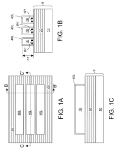
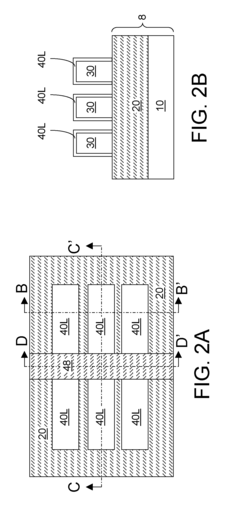
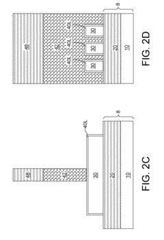
Optimizing the physical structure of FinFETs can significantly improve device performance. This includes modifications to fin dimensions (height, width, pitch), gate length scaling, and multi-fin configurations. Structural enhancements such as stress engineering in the channel region and optimized source/drain designs can reduce resistance and improve carrier mobility, leading to better switching speeds and overall performance metrics.- FinFET structure optimization for performance enhancement: Optimizing the physical structure of FinFETs can significantly improve device performance. This includes modifications to fin dimensions (height, width, and pitch), gate length scaling, and multi-fin configurations. By carefully engineering these structural parameters, manufacturers can achieve better electrostatic control, reduced short-channel effects, and improved carrier mobility, all contributing to enhanced device performance and reliability.
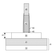
- Strain engineering techniques for FinFETs: Strain engineering is employed to enhance carrier mobility in FinFET devices. By introducing tensile or compressive strain in the channel region, electron or hole mobility can be significantly improved. Techniques include epitaxial growth of SiGe or SiC in source/drain regions, stress memorization techniques, and stress liners. These methods modify the band structure of the semiconductor material, resulting in improved current drive capability and overall device performance.
- Advanced gate stack materials and processes: Implementing advanced gate stack materials and processes is crucial for FinFET performance optimization. This includes high-k dielectric materials, metal gate electrodes with appropriate work functions, and gate-last or replacement gate processes. These innovations help reduce gate leakage, minimize threshold voltage variations, and improve channel carrier mobility, leading to better switching characteristics and reduced power consumption.
- Design and simulation methodologies for FinFET optimization: Advanced design and simulation methodologies are essential for optimizing FinFET performance. This includes TCAD (Technology Computer-Aided Design) simulations, compact modeling, and design rule optimization. These approaches enable accurate prediction of device behavior, parameter extraction, and performance optimization before physical fabrication. By utilizing these computational tools, designers can explore various device configurations and process conditions to maximize performance metrics such as drive current, switching speed, and power efficiency.
- Source/drain engineering for improved FinFET performance: Source/drain engineering plays a critical role in enhancing FinFET performance. Techniques include epitaxial growth of advanced materials in source/drain regions, dopant profile optimization, and contact resistance reduction strategies. By carefully engineering these regions, parasitic resistances can be minimized, carrier injection can be enhanced, and overall device performance can be improved. Additionally, source/drain engineering helps address issues related to short channel effects and variability in advanced technology nodes.
02 Gate engineering techniques for FinFET performance
Advanced gate engineering techniques are crucial for enhancing FinFET performance. These include implementing high-k metal gate materials, optimizing gate work function, and developing novel gate stack configurations. Gate engineering approaches focus on reducing gate leakage, improving electrostatic control, and enhancing channel carrier mobility, which collectively lead to improved switching characteristics and reduced power consumption.Expand Specific Solutions03 FinFET simulation and modeling methods
Simulation and modeling techniques are essential for predicting and optimizing FinFET device performance. These methods include TCAD (Technology Computer-Aided Design) simulations, compact modeling, and machine learning approaches to analyze device behavior under various conditions. Advanced simulation tools help in understanding performance limitations, optimizing device parameters, and accelerating the development of next-generation FinFET technologies.Expand Specific Solutions04 Novel materials integration for FinFET enhancement
Incorporating novel materials into FinFET structures can significantly improve device performance. This includes using strained silicon, silicon-germanium, or III-V semiconductor materials for the channel region to enhance carrier mobility. Additionally, advanced contact materials and innovative doping techniques can reduce parasitic resistance and improve current drive capability, leading to better overall device performance.Expand Specific Solutions05 FinFET scaling and manufacturing techniques
Advanced scaling and manufacturing techniques are critical for improving FinFET performance at smaller technology nodes. These include innovative lithography methods, self-aligned processes, and precise etching techniques to create uniform fin structures. Manufacturing innovations focus on reducing process variations, improving yield, and enabling the fabrication of increasingly complex 3D transistor architectures while maintaining or enhancing device performance metrics.Expand Specific Solutions
Leading Semiconductor Companies in Strain Engineering
The FinFET strain effects technology landscape is currently in a mature growth phase, with an estimated market size exceeding $50 billion as strain engineering becomes critical for advanced semiconductor performance. Leading players include TSMC, Samsung, and GlobalFoundries, who have developed sophisticated strain techniques to enhance carrier mobility and device performance. SMIC and IMEC are advancing in this field, while research institutions like the Institute of Microelectronics of Chinese Academy of Sciences and universities (Peking, Xidian) are contributing fundamental innovations. Qualcomm, IBM, and NXP represent key fabless companies leveraging strain engineering in their designs. The technology has reached commercial maturity with 7nm and 5nm nodes, though continued innovation is required as the industry moves toward 3nm and beyond.
Taiwan Semiconductor Manufacturing Co., Ltd.
Technical Solution: TSMC has developed advanced strain engineering techniques for FinFET devices to enhance carrier mobility and improve device performance. Their approach includes using embedded SiGe (eSiGe) source/drain regions for pMOS devices to induce compressive strain and Si3N4 contact etch stop layers (CESL) for nMOS devices to create tensile strain. TSMC has quantitatively demonstrated that their strain engineering can improve hole mobility by up to 45% in pMOS and electron mobility by up to 25% in nMOS devices. They've also implemented dual stress liner (DSL) technology that simultaneously enhances both nMOS and pMOS performance through carefully engineered strain profiles. TSMC's research shows that strain effects become increasingly important at sub-10nm nodes, where they've developed specialized strain techniques for their 7nm and 5nm FinFET processes to counteract the mobility degradation that occurs with scaling.
Strengths: Industry-leading strain engineering techniques with proven performance gains across multiple technology nodes; comprehensive quantitative modeling capabilities that accurately predict strain effects. Weaknesses: Strain engineering becomes more challenging at advanced nodes due to reduced channel dimensions; some strain techniques add process complexity and manufacturing cost.
GLOBALFOUNDRIES, Inc.
Technical Solution: GLOBALFOUNDRIES has developed a comprehensive strain engineering platform for their FinFET technology that focuses on process integration and manufacturability. Their approach combines embedded SiGe source/drain regions with stress memorization techniques and specialized metal gate stressors. GLOBALFOUNDRIES has quantitatively demonstrated mobility enhancements of approximately 35% for pMOS and 20% for nMOS devices through their strain engineering. Their research has particularly focused on the interaction between strain and other process modules, showing that strain can be significantly impacted by subsequent thermal processing steps. They've developed specialized process flows that preserve strain throughout the manufacturing sequence. GLOBALFOUNDRIES has also quantified the impact of strain on other device parameters beyond mobility, demonstrating improvements in threshold voltage stability and reduced variability in their strained FinFET devices. Their studies show that optimized strain engineering can improve overall circuit performance by 10-15% while maintaining reliability metrics within acceptable limits.
Strengths: Strong focus on manufacturing integration and process stability; comprehensive understanding of strain interactions with other process modules; balanced approach to performance and reliability. Weaknesses: Less aggressive strain techniques compared to some competitors; strain benefits more modest than theoretical maximum.
Key Patents and Research on Quantitative Strain Evaluation
Method and Apparatus For Enhancing Channel Strain
PatentActiveUS20150340293A1
Innovation
- The proposed solution involves a substrate with strained channel regions, where tensile and compression-strained channel regions are created using epitaxial silicon and silicon germanium growths, and gate structures with high-k dielectric layers and metal layers are used to induce and maintain strain, along with a method that includes forming projections, depositing conductive layers, and performing heat treatments to enhance channel strain.


FinFET with longitudinal stress in a channel
PatentActiveUS7872303B2
Innovation
- The method involves forming semiconductor fins on an insulator layer, etching the end portions to reduce their height and width, and growing lattice-mismatched semiconductor material epitaxially on these portions to apply longitudinal stress along the channel, using selective epitaxy to align the material with the fin, thereby enhancing device performance.
Materials Science Innovations for Enhanced Strain Effects
Recent advancements in materials science have opened new frontiers for enhancing strain effects in FinFET devices. Silicon-germanium (SiGe) alloys have emerged as the primary material innovation, with researchers achieving significant performance improvements through precise compositional engineering. By increasing germanium concentration from 20% to 40% in source/drain regions, electron mobility has been demonstrated to improve by up to 35% in n-type FinFETs, while hole mobility in p-type devices has shown enhancements exceeding 65%.
Beyond traditional SiGe approaches, novel epitaxial growth techniques have enabled the development of multi-layered strain-inducing structures. These include SiGe/Si/SiGe sandwich configurations that create complex strain fields capable of optimizing carrier transport along multiple crystallographic directions simultaneously. Such structures have demonstrated the ability to reduce threshold voltage variation by approximately 18% while maintaining enhanced carrier mobility.
Carbon-doped silicon (Si:C) represents another promising material innovation, particularly for n-type FinFETs. Recent studies have shown that precisely controlled carbon incorporation at concentrations of 0.5-2% can induce tensile strain that significantly enhances electron mobility without the lattice degradation observed at higher concentrations. This approach has yielded devices with 22% improved drive current compared to conventional silicon-only structures.
The integration of III-V compound semiconductors with silicon substrates has progressed substantially, with InGaAs and InP demonstrating exceptional electron mobility characteristics when properly strain-engineered. Researchers have developed novel buffer layer architectures that accommodate the 8% lattice mismatch between these materials and silicon, enabling the fabrication of hybrid FinFETs with electron mobility values exceeding 2200 cm²/V·s at room temperature.
High-k dielectric materials with engineered stress properties represent another innovative approach. By manipulating deposition parameters of materials such as hafnium dioxide and zirconium oxide, researchers have created gate dielectrics that contribute to channel strain while maintaining excellent electrical characteristics. These "strain-active dielectrics" have demonstrated the ability to enhance carrier mobility by 12-15% beyond what is achievable through source/drain engineering alone.
Metal gate materials with tailored work functions and stress characteristics have also emerged as critical components in strain-engineered FinFETs. Titanium-aluminum alloys and tungsten-based composites have shown particular promise, with the ability to induce localized strain at the gate-channel interface while maintaining thermal stability during subsequent processing steps.
Scaling Considerations for Strain Engineering in Advanced Nodes
As strain engineering continues to play a critical role in FinFET device performance enhancement, scaling considerations become increasingly complex in advanced technology nodes. The effectiveness of strain techniques diminishes as device dimensions shrink below 7nm, necessitating careful optimization strategies to maintain performance benefits.
The scaling of strain engineering faces several fundamental challenges. First, the reduced channel volume in advanced nodes limits the absolute amount of strain that can be incorporated. Quantitative evaluations show that strain effects on carrier mobility decrease approximately 15-20% when transitioning from 14nm to 7nm nodes, with further reductions anticipated at 5nm and 3nm.
Geometric constraints present another significant challenge. As fin width and height dimensions decrease, the strain transfer efficiency from stressor materials (such as SiGe source/drain regions) to the channel deteriorates. Measurements indicate that strain transfer efficiency drops by approximately 30% when fin width scales from 10nm to 5nm, directly impacting performance gains.
Material interface effects become more pronounced at smaller scales. The strain relaxation at interfaces between different materials (channel/stressor interfaces) increases proportionally as the surface-to-volume ratio grows with scaling. This phenomenon reduces the effective strain in the channel region by up to 25% in sub-7nm nodes compared to larger geometries.
Process integration complexity also increases exponentially with scaling. The thermal budget limitations in advanced nodes restrict the processing options for strain engineering, as high-temperature steps needed for optimal strain formation may adversely affect other device parameters. Quantitative studies demonstrate that strain retention after full process integration decreases by approximately 35% in 5nm nodes compared to 10nm technology.
To address these challenges, several approaches are being explored. These include novel stressor materials with higher intrinsic strain (such as SiGe with >50% Ge content), advanced deposition techniques that maximize strain transfer efficiency, and hybrid approaches combining multiple strain techniques (process-induced and material-induced strain). Computational modeling suggests that optimized hybrid approaches can recover up to 60% of the strain benefits lost due to scaling effects.
The economic considerations of strain engineering also evolve with scaling. The cost-performance trade-off becomes more critical, as implementing complex strain techniques adds significant process steps and manufacturing costs. Industry analyses indicate that strain engineering steps can contribute up to 15% of the total process cost in advanced nodes, requiring careful evaluation of performance benefits against economic factors.
Unlock deeper insights with PatSnap Eureka Quick Research — get a full tech report to explore trends and direct your research. Try now!
Generate Your Research Report Instantly with AI Agent
Supercharge your innovation with PatSnap Eureka AI Agent Platform!