Evaluate FinFET Structural Integrity In Wafer-level Processes
SEP 11, 20259 MIN READ
Generate Your Research Report Instantly with AI Agent
Patsnap Eureka helps you evaluate technical feasibility & market potential.
FinFET Evolution and Structural Integrity Goals
The evolution of FinFET technology represents one of the most significant advancements in semiconductor manufacturing over the past two decades. Beginning with Intel's introduction of tri-gate transistors in 2011, FinFET architecture has enabled the continuation of Moore's Law beyond the physical limitations encountered with planar transistors. The three-dimensional fin structure allows for better electrostatic control of the channel, significantly reducing leakage current and enabling further scaling of transistor dimensions.
As process nodes have shrunk from 22nm to the current 5nm and below, FinFET structures have undergone substantial refinement. Early implementations featured relatively wide, low-aspect-ratio fins, while modern designs incorporate multiple ultra-thin fins with aspect ratios exceeding 10:1. This evolution has introduced increasingly complex structural integrity challenges during wafer-level processing.
The primary goal in evaluating FinFET structural integrity is to ensure mechanical stability throughout the manufacturing process. Fins must withstand numerous thermal cycles, chemical treatments, and mechanical stresses without deformation, cracking, or collapse. Even nanometer-scale deviations can significantly impact electrical performance, particularly as fin widths approach sub-10nm dimensions.
Another critical objective is maintaining consistent fin geometry across the entire wafer. Process-induced variations in fin height, width, or sidewall angle directly translate to transistor performance variability. As circuit designers push for tighter performance specifications, the tolerance for structural variations has decreased dramatically, necessitating more sophisticated evaluation methodologies.
Interface integrity between the fin and surrounding materials represents another key concern. The fin-gate oxide interface must remain defect-free to prevent reliability issues, while the fin-substrate junction requires perfect crystallinity to minimize leakage. Evaluation techniques must therefore assess not only the fin itself but also these critical interfaces.
With the industry transition toward gate-all-around (GAA) and nanosheet architectures, understanding the structural evolution of FinFETs becomes even more valuable. Many of the lessons learned in maintaining FinFET structural integrity directly inform the development of these next-generation technologies, which face even more stringent dimensional control requirements.
The ultimate goal of structural integrity evaluation is to establish robust process windows that maximize yield while maintaining performance targets. This requires developing comprehensive metrology solutions capable of detecting subtle structural variations at high throughput, combined with physics-based models that can predict the impact of these variations on device performance and reliability.
Market Demand for Reliable FinFET Devices
The semiconductor industry's demand for reliable FinFET devices has been growing exponentially as these transistors have become the backbone of modern computing systems. Market research indicates that the global FinFET technology market is projected to reach $50 billion by 2027, with a compound annual growth rate of approximately 22% from 2021. This substantial growth is primarily driven by the increasing adoption of FinFET technology in high-performance computing applications, smartphones, and data centers.
The evaluation of FinFET structural integrity during wafer-level processes has become a critical market requirement as device dimensions continue to shrink below 10nm. Manufacturing stakeholders are increasingly concerned with yield rates, which directly impact production costs and market competitiveness. Industry reports suggest that even minor structural defects in FinFET architecture can reduce yield rates by 15-30%, translating to millions of dollars in lost revenue for semiconductor manufacturers.
Consumer electronics companies, particularly smartphone manufacturers, are demanding more reliable FinFET devices to support advanced features while maintaining battery efficiency. The mobile processor market alone represents approximately 40% of the total demand for FinFET technology, with stringent requirements for structural integrity to ensure consistent performance across millions of devices.
Data center operators and cloud service providers constitute another significant market segment demanding reliable FinFET devices. With the exponential growth in cloud computing and AI applications, these operators require processors that can maintain structural integrity under intensive computational loads. Market surveys indicate that data center operators are willing to pay premium prices for semiconductor components with proven reliability metrics, creating a strong economic incentive for improved FinFET structural evaluation methods.
Automotive and industrial IoT applications represent emerging markets for FinFET technology, with particularly stringent requirements for structural integrity. These applications often operate in harsh environmental conditions and require extended operational lifespans of 10-15 years, compared to the 2-5 year lifecycle of consumer electronics. The automotive semiconductor market is expected to grow at 25% annually through 2026, with advanced driver assistance systems and autonomous driving features creating new demand for highly reliable FinFET devices.
The geographical distribution of market demand shows concentration in East Asia for manufacturing, North America for design innovation, and growing demand in emerging markets as digital infrastructure expands globally. This global market landscape underscores the universal need for improved methods to evaluate and ensure FinFET structural integrity during wafer-level processes.
Current Challenges in FinFET Wafer-level Processing
The semiconductor industry's continuous pursuit of Moore's Law has led to the development of FinFET technology, which has become the cornerstone of modern integrated circuit manufacturing. However, as device dimensions shrink below 10nm, ensuring the structural integrity of FinFETs during wafer-level processes presents significant challenges that demand innovative solutions.
One of the primary challenges is maintaining fin geometry consistency across the wafer. Process variations in etching, deposition, and planarization can lead to non-uniform fin heights, widths, and pitches. These variations directly impact device performance parameters such as threshold voltage, leakage current, and on-state current. Recent studies indicate that even a 1nm variation in fin width can result in up to 15% fluctuation in device performance metrics.
Mechanical stress management has emerged as another critical challenge. During wafer-level processes, thermal cycling and material deposition create significant mechanical stresses that can deform the delicate fin structures. These stresses are particularly problematic at the fin-substrate interface and can lead to fin bending, cracking, or even complete structural failure. The industry is actively developing stress-compensation techniques and novel materials with matched thermal expansion coefficients to mitigate these issues.
Aspect ratio dependent etching (ARDE) effects become increasingly pronounced as fin dimensions decrease. The etching chemistry and plasma conditions must be precisely controlled to ensure uniform etching rates regardless of feature size and density. Manufacturers are implementing advanced etching techniques such as atomic layer etching (ALE) and cyclic etch-passivation processes to achieve the required precision, but these approaches significantly increase process complexity and cost.
Defect management presents another formidable challenge. As fin dimensions approach atomic scales, even nanoscale defects can critically impact device functionality. Defects such as line edge roughness (LER), line width roughness (LWR), and random dopant fluctuations (RDF) become increasingly difficult to control. Advanced metrology techniques including high-resolution TEM, AFM, and optical scatterometry are being deployed for defect detection, but in-line monitoring remains challenging.
Integration with subsequent process steps introduces additional complexities. Gate stack formation, spacer creation, and source/drain epitaxy must be performed without compromising fin integrity. The industry is exploring selective deposition techniques and atomic layer precision processes to address these integration challenges, but yield and reliability concerns persist.
Finally, the economic viability of increasingly complex wafer-level processes poses a significant challenge. The capital expenditure for advanced FinFET manufacturing facilities now exceeds $10 billion, with process control equipment accounting for a substantial portion of this investment. Balancing technological advancement with economic constraints requires careful optimization of process flows and equipment utilization.
Existing Methodologies for FinFET Structural Evaluation
01 FinFET structural design optimization
Optimization of FinFET structures involves specific design parameters to enhance structural integrity. This includes fin geometry modifications, gate structure reinforcement, and material selection to prevent deformation and stress-induced failures. These design optimizations help maintain device performance while ensuring mechanical stability under various operational conditions.- FinFET structural design optimization: Various design approaches can be implemented to enhance the structural integrity of FinFET devices. These include optimizing fin geometry, gate structure modifications, and material selection to improve mechanical stability. Advanced modeling techniques help predict stress distribution and potential failure points, allowing for preemptive design adjustments that enhance overall device reliability while maintaining electrical performance characteristics.
- Stress testing and structural analysis methods: Specialized testing methodologies have been developed to evaluate the structural integrity of FinFET devices under various operational conditions. These include thermal cycling tests, mechanical stress analysis, and vibration testing to identify potential failure modes. Advanced analytical techniques help quantify the resilience of FinFET structures and predict their long-term reliability, enabling manufacturers to implement appropriate reinforcement measures where necessary.
- Material selection for enhanced durability: The choice of materials significantly impacts the structural integrity of FinFET devices. High-quality semiconductor materials, specialized dielectrics, and reinforced gate materials can substantially improve mechanical strength and thermal stability. Composite materials and novel alloys are being explored to enhance resistance to mechanical deformation, thermal expansion, and environmental degradation, thereby extending device lifespan and reliability.
- Manufacturing process controls for structural integrity: Precise manufacturing process controls are essential for ensuring the structural integrity of FinFET devices. This includes optimized etching techniques, deposition parameters, and thermal treatment protocols that minimize structural defects. In-line monitoring systems and quality control measures help identify potential structural weaknesses during fabrication, allowing for immediate corrective actions to maintain the mechanical stability of the final devices.
- Packaging solutions for FinFET protection: Advanced packaging technologies play a crucial role in protecting FinFET structures from external mechanical stresses and environmental factors. Specialized encapsulation materials, stress buffer layers, and reinforced interconnect designs help distribute mechanical forces and prevent structural damage. These packaging solutions are designed to shield the delicate fin structures while facilitating efficient heat dissipation and electrical connectivity, thereby preserving the structural integrity throughout the device lifetime.
02 Stress management in FinFET fabrication
Managing stress in FinFET structures is crucial for maintaining structural integrity. Techniques include stress-relief layers, buffer materials, and controlled deposition processes to minimize mechanical strain. These approaches help prevent fin cracking, delamination, and other stress-related failures that could compromise device functionality and reliability.Expand Specific Solutions03 Testing methods for FinFET structural integrity
Various testing methodologies are employed to evaluate and ensure FinFET structural integrity. These include non-destructive testing techniques, simulation-based stress analysis, and accelerated aging tests to identify potential failure modes. Advanced imaging and measurement systems help detect structural weaknesses before they lead to device failure.Expand Specific Solutions04 Thermal stability enhancement for FinFETs
Thermal management is essential for maintaining FinFET structural integrity during operation. Techniques include thermal dissipation structures, heat-resistant materials, and thermal boundary engineering to prevent temperature-induced deformation. These approaches help maintain device performance and reliability under varying thermal conditions.Expand Specific Solutions05 Environmental protection for FinFET structures
Protecting FinFET structures from environmental factors is critical for long-term structural integrity. This includes encapsulation techniques, moisture barriers, and contamination prevention methods to shield sensitive components from external damage. These protective measures help extend device lifespan and maintain performance reliability in various operating environments.Expand Specific Solutions
Leading Semiconductor Manufacturers and Equipment Providers
The FinFET structural integrity evaluation market is currently in a growth phase, with increasing demand driven by advanced semiconductor manufacturing processes. The global market size is estimated to exceed $2 billion, expanding at approximately 8-10% annually as chipmakers push toward smaller nodes. Leading players include TSMC and GlobalFoundries, who have established mature FinFET evaluation technologies, while SMIC, Huahong Grace, and UMC are rapidly advancing their capabilities. Research institutions like IMEC and Institute of Microelectronics of Chinese Academy of Sciences provide critical innovation support. Equipment suppliers such as Applied Materials offer specialized tools for structural integrity assessment. The competitive landscape is characterized by intense R&D investment as companies strive to address challenges in 7nm and below processes, with collaboration between IDMs, foundries, and equipment vendors becoming increasingly important.
Taiwan Semiconductor Manufacturing Co., Ltd.
Technical Solution: TSMC has developed a comprehensive multi-faceted approach to evaluate FinFET structural integrity during wafer-level processes. Their methodology combines advanced metrology techniques with in-line monitoring systems. TSMC employs high-resolution scanning electron microscopy (SEM) and transmission electron microscopy (TEM) for physical inspection of fin structures, allowing detection of defects as small as 1-2nm. They've implemented optical scatterometry and X-ray diffraction techniques to measure critical dimensions and assess strain in FinFET structures non-destructively. TSMC's proprietary process control system integrates real-time data from multiple inspection points to create a holistic view of structural integrity across the wafer. Their approach includes electrical parameter testing through specialized test structures embedded in scribe lines, enabling correlation between physical defects and electrical performance. TSMC has also pioneered the use of machine learning algorithms to predict potential structural failures based on historical process data and inspection results.
Strengths: Industry-leading metrology capabilities with sub-nanometer resolution; integrated approach combining physical, optical and electrical testing; advanced data analytics for predictive quality control. Weaknesses: High capital investment required for comprehensive inspection systems; complex data integration challenges across different inspection methodologies; trade-off between inspection coverage and production throughput.
International Business Machines Corp.
Technical Solution: IBM has developed a multi-modal approach to FinFET structural integrity evaluation focusing on non-destructive testing methodologies. Their system employs a combination of electrical and physical characterization techniques. IBM's approach begins with advanced electrical testing that can detect subtle variations in transistor performance indicative of structural issues. They've pioneered specialized test structures that amplify the electrical signatures of specific defect types. For physical characterization, IBM utilizes atomic force microscopy (AFM) techniques that can map the three-dimensional profile of fin structures with nanometer precision. Their proprietary image processing algorithms can automatically identify deviations from ideal fin geometry. IBM has also developed novel acoustic microscopy techniques that can detect subsurface defects and delamination within the FinFET structure without damaging the wafer. Their system integrates these multiple data streams through a unified analysis platform that correlates electrical anomalies with physical defects, enabling root cause analysis of structural integrity issues.
Strengths: Exceptional non-destructive testing capabilities; sophisticated correlation between electrical and physical defect signatures; advanced data integration platform. Weaknesses: Some techniques have limited throughput for high-volume manufacturing; requires highly specialized expertise to interpret complex multi-modal data; higher cost per wafer for comprehensive analysis.
Critical Patents in FinFET Structural Integrity Assessment
Fin-shaped field-effect transistor process
PatentActiveUS20150380319A1
Innovation
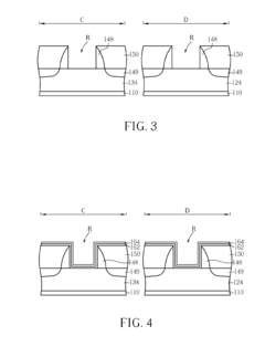
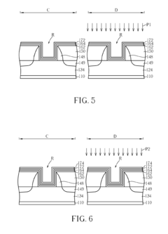
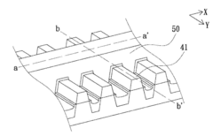
- A fin-shaped field-effect transistor process that involves a treatment process to adjust the physical and chemical properties of metal layers, such as the work function value, to enhance the threshold voltage and overall electrical performance.
Fin field effect transistor device and fabrication method thereof
PatentActiveUS20160163837A1
Innovation
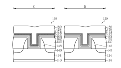
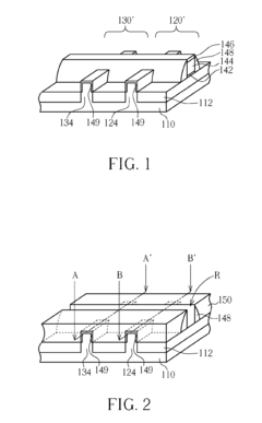
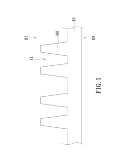
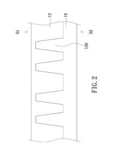
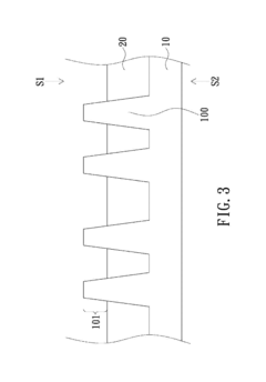
- A method for fabricating a FinFET device involving the formation of a substrate with a fin structure, an oxide layer, shallow trench isolation, spacers, and an epitaxial fin structure, where the gate structure is perpendicular to the epitaxial fin, and the epitaxial fin can be made of germanium with varying compositions, allowing for improved electrical control and efficiency.
Yield Optimization Strategies for FinFET Manufacturing
Yield optimization in FinFET manufacturing represents a critical focus area for semiconductor fabrication facilities seeking to maximize production efficiency and device performance. The implementation of comprehensive statistical process control (SPC) systems enables real-time monitoring of key process parameters, allowing for immediate intervention when deviations occur. These systems track critical dimensions, film thicknesses, and electrical characteristics throughout the manufacturing process, providing valuable data for continuous improvement initiatives.
Advanced metrology techniques play a pivotal role in yield optimization by enabling precise measurement of fin dimensions, gate profiles, and other critical features. Optical critical dimension (OCD) metrology, scanning electron microscopy (SEM), and atomic force microscopy (AFM) provide complementary data sets that, when integrated, offer a comprehensive view of structural integrity across the wafer surface.
Process window optimization represents another essential strategy, involving the systematic exploration of process parameters to identify robust operating conditions. This approach typically employs design of experiments (DOE) methodologies to efficiently map the relationship between process variables and device performance metrics. The resulting process windows define the acceptable ranges for parameters such as exposure dose, focus settings, etch times, and deposition conditions.
Defect reduction initiatives focus on identifying and eliminating sources of structural failures in FinFET devices. Particle control in clean room environments, chemical purity management, and equipment maintenance protocols all contribute to minimizing defect densities. Advanced inspection tools, including brightfield and darkfield optical systems, e-beam inspection, and voltage contrast techniques, enable detection of increasingly subtle defects that can compromise fin structure.
Integration of machine learning algorithms with manufacturing data streams has emerged as a powerful approach for yield prediction and enhancement. These systems analyze historical process data to identify complex patterns and correlations that may not be apparent through traditional statistical methods. Predictive models can anticipate yield issues before they manifest, allowing for preemptive adjustments to process parameters.
Thermal budget management represents a critical consideration for maintaining FinFET structural integrity. Careful control of thermal processes, including annealing steps, implant activation, and deposition temperatures, helps preserve fin geometry and prevent unwanted diffusion or reflow of materials. Advanced rapid thermal processing (RTP) systems with precise temperature control capabilities support this objective.
Cross-functional yield management teams, bringing together expertise from process engineering, equipment engineering, and quality assurance, provide the organizational framework necessary for sustained yield improvement. These teams coordinate root cause analysis activities and implement corrective actions when yield excursions occur.
Environmental Impact of Advanced Node Fabrication
The environmental footprint of advanced node fabrication, particularly in FinFET manufacturing processes, represents a significant concern for the semiconductor industry. As process nodes shrink below 10nm, the environmental impact intensifies due to increased resource consumption, chemical usage, and energy requirements. FinFET production specifically demands ultra-pure water in quantities that exceed 1,000 gallons per wafer, creating substantial water management challenges in regions already facing scarcity issues.
Chemical usage in advanced node fabrication presents another environmental challenge. The etching and cleaning processes for creating the complex three-dimensional FinFET structures require highly specialized chemicals, many of which have significant global warming potential or contribute to air quality degradation. Perfluorocompounds (PFCs) and sulfur hexafluoride (SF6), commonly used in plasma etching processes, possess global warming potentials thousands of times greater than carbon dioxide.
Energy consumption represents perhaps the most substantial environmental impact factor. The extreme precision required for FinFET structural integrity verification demands sophisticated metrology equipment and cleanroom environments operating continuously. A typical advanced semiconductor fabrication facility consumes electricity equivalent to approximately 50,000 households, with the majority directed toward maintaining the controlled manufacturing environment rather than actual production processes.
Waste management presents additional challenges unique to advanced node fabrication. The complex multi-layer processes generate substantial amounts of chemical waste, including heavy metals and toxic compounds that require specialized treatment. The industry has made progress in recycling certain materials, particularly expensive metals like copper and cobalt, but comprehensive recycling solutions remain elusive for many process chemicals.
Regulatory frameworks worldwide are increasingly focusing on the semiconductor industry's environmental impact. The European Union's Restriction of Hazardous Substances (RoHS) directive and similar regulations in Asia have pushed manufacturers to develop alternative processes with reduced environmental footprints. Leading semiconductor companies have responded by establishing ambitious sustainability targets, including commitments to carbon neutrality and significant reductions in water usage by 2030.
Technological innovations offer promising pathways to mitigate these environmental impacts. Dry etching techniques that reduce chemical usage, advanced water recycling systems achieving over 90% reuse rates, and energy-efficient facility designs are becoming industry standards. Additionally, improvements in yield management directly contribute to environmental sustainability by reducing resource waste through more efficient manufacturing processes.
Unlock deeper insights with Patsnap Eureka Quick Research — get a full tech report to explore trends and direct your research. Try now!
Generate Your Research Report Instantly with AI Agent
Supercharge your innovation with Patsnap Eureka AI Agent Platform!
