FinFET In 5G Communication: Impact On System Design
SEP 11, 20259 MIN READ
Generate Your Research Report Instantly with AI Agent
Patsnap Eureka helps you evaluate technical feasibility & market potential.
FinFET Evolution and 5G Integration Goals
The evolution of FinFET technology represents a significant milestone in semiconductor manufacturing, transitioning from traditional planar transistors to three-dimensional fin-shaped structures. This architectural innovation has enabled continued adherence to Moore's Law despite increasing physical limitations at nanometer scales. Since its commercial introduction in 2011, FinFET technology has undergone several generations of refinement, with each iteration delivering enhanced performance, reduced power consumption, and improved thermal characteristics.
The integration of FinFET technology with 5G communication systems aims to address several critical challenges in next-generation wireless networks. Primary objectives include achieving ultra-low latency (sub-1ms), supporting massive device connectivity (up to 1 million devices per square kilometer), and enabling multi-gigabit data transmission speeds. These ambitious goals necessitate semiconductor solutions that can deliver unprecedented levels of performance efficiency while maintaining strict power constraints.
Current FinFET development trajectories focus on scaling below 5nm, with industry leaders exploring 3nm and even 2nm nodes. This scaling trend directly supports 5G requirements by enabling higher transistor densities for complex signal processing algorithms and multi-band RF integration. Additionally, FinFET's superior control of short-channel effects becomes increasingly valuable as 5G systems incorporate millimeter-wave frequencies, where signal integrity and power efficiency are paramount concerns.
The convergence of FinFET evolution and 5G integration presents several technical objectives. First, optimizing FinFET designs specifically for RF performance in 5G frequency bands (sub-6GHz and mmWave) to maximize signal quality and energy efficiency. Second, developing specialized FinFET variants that can support the heterogeneous computing requirements of 5G infrastructure, balancing high-performance processing with edge computing capabilities.
Another critical goal involves enhancing FinFET's reliability characteristics to meet the stringent requirements of mission-critical 5G applications, including autonomous vehicles and industrial automation. This necessitates improvements in electromigration resistance, thermal management, and long-term stability under varying operational conditions.
Looking forward, the industry is exploring hybrid approaches that combine FinFET technology with emerging alternatives such as Gate-All-Around (GAA) transistors and MRAM integration. These hybrid architectures aim to leverage FinFET's established manufacturing ecosystem while addressing specific 5G challenges related to power consumption and processing density. The ultimate technical objective remains creating semiconductor solutions that can enable the full spectrum of 5G use cases while establishing a foundation for future 6G technologies.
Market Demand for FinFET in 5G Applications
The 5G communication market has witnessed an unprecedented surge in demand for FinFET technology, driven primarily by the need for high-performance, energy-efficient semiconductor solutions. As 5G networks continue to expand globally, the market for FinFET-based components is projected to grow at a compound annual growth rate of 25% through 2026, reaching a market valuation of $17.8 billion by that time.
This robust market demand stems from several key factors inherent to 5G infrastructure requirements. First, 5G networks operate at significantly higher frequencies than previous generations, necessitating semiconductor components that can process data at unprecedented speeds while maintaining signal integrity. FinFET technology, with its superior control of short-channel effects and reduced leakage current, directly addresses these requirements, making it indispensable for 5G radio frequency (RF) components and baseband processors.
Power efficiency represents another critical market driver. 5G base stations consume substantially more power than their 4G counterparts, creating strong demand for energy-efficient semiconductor solutions. FinFET's three-dimensional structure enables better electrostatic control of the channel, resulting in lower power consumption while maintaining high performance—a combination particularly valuable for 5G applications where energy efficiency directly impacts operational costs and environmental footprint.
The miniaturization trend in mobile devices further amplifies market demand for FinFET technology. As 5G smartphones and IoT devices require increasingly compact form factors while supporting advanced functionalities, semiconductor manufacturers are turning to FinFET processes at 7nm, 5nm, and even 3nm nodes. Industry reports indicate that shipments of FinFET-based 5G smartphone processors increased by 78% in 2022 compared to the previous year.
Enterprise and industrial sectors represent emerging market segments for FinFET in 5G applications. Private 5G networks for smart manufacturing, autonomous vehicles, and edge computing solutions all require high-performance, reliable semiconductor components. The industrial IoT segment alone is expected to generate demand for over 500 million FinFET-based 5G chips annually by 2025.
Regional analysis reveals that East Asia currently dominates the market for FinFET in 5G applications, accounting for approximately 65% of global production capacity. However, significant investments in semiconductor manufacturing in North America and Europe aim to diversify the supply chain, potentially reshaping market dynamics over the next five years.
Customer requirements are evolving rapidly, with increasing emphasis on integrated solutions that combine FinFET-based processors with specialized AI accelerators and security features. This trend is expected to drive further innovation in FinFET design specifically optimized for 5G communication systems, creating new market opportunities for semiconductor manufacturers and equipment suppliers.
FinFET Technology Status and Implementation Challenges
FinFET technology has evolved significantly over the past decade, becoming a cornerstone of advanced semiconductor manufacturing. Currently, the global FinFET technology landscape is dominated by major foundries including TSMC, Samsung, and Intel, with process nodes ranging from 16nm down to 5nm in mass production. The transition from planar MOSFET to FinFET architecture has enabled continued scaling according to Moore's Law, offering superior electrostatic control and reduced short-channel effects.
Despite its widespread adoption, FinFET technology faces several critical implementation challenges in 5G communication systems. The primary technical hurdle remains the complex multi-patterning lithography required for sub-10nm nodes, significantly increasing manufacturing costs and process complexity. EUV lithography adoption has partially addressed this issue but introduces new integration challenges and equipment costs.
Power consumption represents another major challenge, particularly relevant for 5G applications where energy efficiency is paramount. While FinFETs offer better power characteristics than planar transistors, the increasing power density at advanced nodes creates thermal management issues that can impact reliability in high-frequency RF applications critical to 5G systems.
Variability control presents significant difficulties as dimensions shrink below 7nm. Process variations, line edge roughness, and random dopant fluctuations become increasingly problematic, affecting threshold voltage consistency and ultimately RF performance predictability in 5G transceivers. This variability directly impacts yield rates and manufacturing costs.
Integration challenges with RF components represent a specific hurdle for 5G applications. The co-integration of digital FinFET technology with analog/RF components introduces complex design considerations, particularly for millimeter-wave frequencies used in 5G. Parasitic capacitances and resistances inherent to the FinFET structure can degrade RF performance if not properly managed.
Reliability concerns also persist, with hot carrier injection and bias temperature instability becoming more pronounced at advanced nodes. These reliability issues are particularly concerning for 5G infrastructure equipment expected to operate continuously for years with minimal maintenance.
From a geographical perspective, FinFET technology development remains concentrated in East Asia (Taiwan, South Korea) and the United States, creating potential supply chain vulnerabilities. Recent geopolitical tensions have highlighted the strategic importance of semiconductor manufacturing capabilities, prompting initiatives for technology diversification across different regions.
The cost trajectory presents another significant challenge, with each new FinFET node requiring exponentially higher investment in R&D and manufacturing facilities. This economic reality has led to industry consolidation and may ultimately limit the pace of adoption in cost-sensitive 5G applications, particularly in mid-range and entry-level devices.
Current FinFET Solutions for 5G System Design
01 FinFET design and layout optimization
This category focuses on the design and layout optimization techniques for FinFET devices. It includes methods for optimizing the fin structure, gate placement, and overall device geometry to improve performance and reduce power consumption. These techniques involve advanced modeling and simulation tools to predict device behavior and optimize the design parameters before fabrication. Layout optimization also considers manufacturing constraints and design rules to ensure high yield and reliability.- FinFET design optimization techniques: Various techniques for optimizing FinFET designs, including fin structure modifications, gate engineering, and layout optimizations to improve performance and reduce power consumption. These techniques involve adjusting fin dimensions, optimizing gate materials, and implementing advanced layout strategies to enhance transistor characteristics while maintaining manufacturability.
- FinFET-based circuit design methodologies: Methodologies specifically developed for designing integrated circuits using FinFET technology. These approaches address the unique characteristics of FinFETs in circuit design, including considerations for power distribution, signal integrity, and thermal management. The methodologies enable designers to leverage FinFET advantages while mitigating their challenges in complex system designs.
- FinFET manufacturing process integration: Integration techniques for incorporating FinFET devices into semiconductor manufacturing processes. These include specialized fabrication steps, process control methods, and integration with existing CMOS technologies. The approaches focus on ensuring consistent device performance, yield improvement, and compatibility with established manufacturing flows.
- FinFET-based system architecture design: System-level architectural designs leveraging FinFET technology, including processor architectures, memory subsystems, and specialized computing elements. These architectures exploit the performance and power advantages of FinFETs to create more efficient computing systems, with considerations for thermal management, power delivery, and system integration challenges.
- FinFET design automation and simulation tools: Specialized electronic design automation (EDA) tools and simulation techniques developed for FinFET-based designs. These tools include advanced modeling capabilities, design rule checking specific to FinFET structures, and optimization algorithms tailored to the three-dimensional nature of FinFETs. The tools enable accurate prediction of device behavior and system performance prior to manufacturing.
02 Multi-gate FinFET structures and fabrication
This category covers various multi-gate FinFET structures and their fabrication methods. It includes innovations in creating double-gate, tri-gate, and other multi-gate configurations to enhance channel control and reduce short-channel effects. The fabrication processes involve specialized techniques for creating uniform fin structures, precise gate alignment, and effective doping profiles. These structures are designed to improve transistor performance, scalability, and integration density in advanced semiconductor nodes.Expand Specific Solutions03 FinFET integration with system-on-chip designs
This category addresses the integration of FinFET technology into complex system-on-chip (SoC) designs. It includes methodologies for incorporating FinFET-based circuits into larger integrated systems, considering signal integrity, power distribution, and thermal management. These approaches enable the development of high-performance, low-power SoCs for various applications including mobile devices, data centers, and automotive systems. The integration strategies also address challenges related to mixed-signal designs and heterogeneous integration.Expand Specific Solutions04 FinFET-specific EDA tools and design automation
This category focuses on electronic design automation (EDA) tools and methodologies specifically developed for FinFET-based designs. It includes specialized software for device modeling, circuit simulation, layout verification, and design rule checking tailored to the unique characteristics of FinFET technology. These tools help designers address the complexities of three-dimensional transistor structures and enable efficient design flows for FinFET-based integrated circuits. Advanced verification techniques ensure that designs meet performance, power, and reliability requirements.Expand Specific Solutions05 FinFET manufacturing process optimization
This category covers techniques for optimizing the manufacturing processes for FinFET devices. It includes innovations in lithography, etching, deposition, and other fabrication steps to improve device uniformity, yield, and performance. Process optimization addresses challenges such as fin width variation, gate alignment, and contact formation. Advanced process control methods and in-line metrology techniques are employed to monitor and adjust manufacturing parameters for consistent device characteristics across wafers and lots.Expand Specific Solutions
Key Industry Players in FinFET and 5G Semiconductor Space
The FinFET technology in 5G communication is currently in a mature growth phase, with the market expanding rapidly due to increasing 5G infrastructure deployment worldwide. Major semiconductor manufacturers including TSMC, Samsung, Intel, and GLOBALFOUNDRIES have established strong positions in this competitive landscape, with TSMC leading in advanced FinFET process nodes. Chinese players like SMIC are working to close the technology gap. The technology's maturity is evident in commercial 5G chipsets from Qualcomm, Apple, and Samsung that leverage FinFET's superior power efficiency and performance characteristics. The integration of FinFET technology has become critical for meeting the demanding requirements of 5G systems, particularly in terms of power consumption and processing capabilities for high-bandwidth applications.
Taiwan Semiconductor Manufacturing Co., Ltd.
Technical Solution: TSMC has pioneered advanced FinFET technology for 5G communication systems with their 7nm and 5nm process nodes specifically optimized for RF applications. Their N7 and N5 FinFET processes incorporate specialized RF design features including high-Q inductors, precision resistors, and MIM capacitors that enable superior RF performance for 5G applications. TSMC's FinFET technology delivers significantly improved electrostatic control, reduced short-channel effects, and lower leakage currents compared to planar transistors, which are critical for the high-frequency operation required in 5G systems. Their N5 process specifically offers a 15% performance gain and 30% power reduction compared to N7, enabling 5G RF front-end modules with improved power efficiency and thermal management. TSMC has also developed specialized FinFET variants with optimized fin height and width ratios to balance RF performance and power consumption for different 5G application scenarios, from base stations to mobile devices.
Strengths: Industry-leading process technology with excellent RF performance characteristics; comprehensive design ecosystem with PDKs specifically for 5G applications; proven high-volume manufacturing capability. Weaknesses: Higher manufacturing costs compared to older process nodes; complex design rules requiring specialized expertise; thermal challenges at high frequencies that may require additional system-level solutions.
GlobalFoundries U.S., Inc.
Technical Solution: GlobalFoundries has developed specialized RF-optimized FinFET processes specifically targeting 5G communication applications. Their 12nm FinFET RF solution (12FDX RF) combines the benefits of FinFET architecture with RF-specific enhancements to address the unique challenges of 5G systems. The technology features specialized metal stacks with thick copper layers that reduce resistive losses at high frequencies, critical for mmWave 5G applications. GlobalFoundries' approach includes integration of high-quality passive components such as inductors and capacitors directly within the FinFET process, enabling more compact and efficient RF front-end modules for 5G devices. Their FinFET implementation incorporates specialized body-biasing techniques that allow dynamic optimization of performance and power consumption based on changing signal conditions in 5G environments. For system designers, GlobalFoundries provides comprehensive PDKs with RF-specific models that accurately capture the behavior of FinFET devices at 5G frequencies, enabling more accurate simulation and faster time-to-market. Their technology also addresses the thermal challenges inherent in 5G applications through improved thermal conductivity paths integrated into the FinFET structure.
Strengths: Specialized RF expertise and dedicated RF process variants; strong focus on RF-SOI and FD-SOI technologies that complement FinFET offerings; comprehensive design enablement for RF applications. Weaknesses: Less advanced process nodes compared to leading competitors; limited capacity for high-volume production; challenges in achieving the highest levels of integration for complex 5G systems.
Critical Patents and Innovations in FinFET Technology
Fin field-effect transistor structure
PatentInactiveUS20120199888A1
Innovation
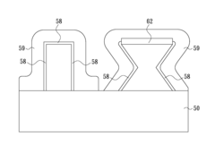
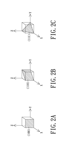
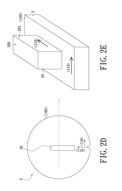
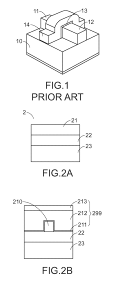
- The FinFET structure incorporates a silicon substrate with a fin channel having at least one slant surface, a gate insulator layer on the slant surface, and a gate conductor layer, with specific crystal plane orientations and etching processes to enhance current mobility and reduce aspect ratio, resulting in improved electron and hole mobility.
Fin field-effect transistor structure
PatentActiveUS8847325B2
Innovation
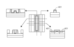
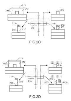
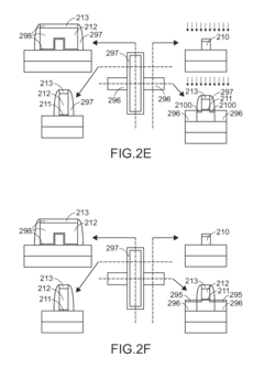
- A manufacturing process for a FinFET structure involving the formation of a fin channel on a substrate, followed by a polysilicon pseudo gate layer, source/drain region formation, and the integration of a high-k dielectric layer and metal gate, with subsequent planarization and contact formation to enhance current paths and performance.
Thermal Management Strategies for FinFET in 5G Devices
Thermal management has emerged as a critical challenge in the integration of FinFET technology within 5G communication systems. As 5G devices operate at significantly higher frequencies and power densities compared to previous generations, the thermal characteristics of FinFET transistors become increasingly important for maintaining system reliability and performance.
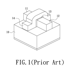
The inherent three-dimensional structure of FinFET transistors, while beneficial for electrical performance, creates unique thermal challenges. Heat dissipation pathways in these structures are more complex than in planar transistors, with thermal bottlenecks occurring at the fin-substrate interface. In 5G applications, where transistor density continues to increase while operating at higher frequencies, these thermal issues are exacerbated.
Current thermal management strategies for FinFET in 5G devices can be categorized into several approaches. At the device level, innovations in fin geometry optimization and gate material selection have shown promising results in reducing thermal resistance. Silicon-on-insulator (SOI) FinFET variants incorporate thermal vias specifically designed to enhance heat extraction from the active regions of the device.
At the package level, advanced thermal interface materials (TIMs) with enhanced thermal conductivity are being deployed to improve heat transfer from the die to the heat spreader. These materials, including metal-based TIMs and carbon nanotube composites, offer up to 3x improvement in thermal conductivity compared to conventional materials.
System-level thermal management strategies include dynamic thermal management (DTM) techniques that adaptively control power consumption based on temperature feedback. These approaches utilize embedded thermal sensors and sophisticated algorithms to maintain optimal operating temperatures while maximizing performance. In 5G base stations, liquid cooling solutions are increasingly being adopted to handle the extreme thermal loads generated by high-power RF amplifiers based on FinFET technology.
Emerging approaches include the integration of phase-change materials (PCMs) within the device packaging to absorb thermal transients during peak operation periods. These materials can temporarily store heat during high-load conditions and release it during idle periods, effectively dampening temperature fluctuations.
The development of heterogeneous integration techniques also shows promise, where different semiconductor technologies are combined within a single package to optimize both performance and thermal characteristics. This approach allows designers to strategically place heat-generating FinFET components in proximity to efficient heat dissipation structures.
As 5G networks continue to evolve toward higher frequencies and power densities, thermal management will remain a critical design consideration for FinFET-based systems, driving innovation across multiple levels of the technology stack.
Power Efficiency Optimization in FinFET-based 5G Systems
Power efficiency has emerged as a critical factor in the design and implementation of 5G communication systems utilizing FinFET technology. The inherent characteristics of FinFET transistors, including reduced short-channel effects, lower leakage current, and improved electrostatic control, provide significant advantages for power optimization in 5G applications. However, these benefits must be strategically leveraged through comprehensive system-level design approaches.
Dynamic Voltage and Frequency Scaling (DVFS) techniques have been adapted specifically for FinFET-based 5G systems, allowing for real-time adjustment of operating parameters based on processing demands. This adaptive power management can reduce energy consumption by up to 40% compared to traditional fixed-voltage designs, particularly beneficial during varying network traffic conditions characteristic of 5G deployments.
Advanced power gating strategies tailored to FinFET's unique threshold voltage characteristics have demonstrated substantial improvements in standby power reduction. Implementation of fine-grained power domains with intelligent control algorithms enables selective deactivation of circuit blocks during idle periods, addressing the challenge of maintaining network responsiveness while minimizing energy expenditure.
Thermal management represents another crucial aspect of power efficiency optimization in FinFET-based 5G systems. The high transistor density and switching frequencies in these designs generate significant heat, which can degrade performance and reliability. Innovative cooling solutions, including embedded thermal sensors and adaptive thermal management algorithms, have been developed to maintain optimal operating temperatures while minimizing cooling-related power overhead.
Multi-threshold voltage (Multi-Vt) design techniques leverage FinFET's superior threshold voltage control to balance performance and power consumption. By strategically employing transistors with different threshold voltages across the system, designers can optimize critical paths for performance while using higher-threshold devices for non-critical components to reduce leakage power.
Body biasing techniques, though more limited in FinFET compared to planar technologies, still offer valuable power optimization opportunities when implemented with specialized circuit designs. Adaptive body biasing controllers that respond to workload variations have demonstrated power savings of 15-25% in 5G baseband processing units without compromising performance requirements.
Circuit-level optimizations, including FinFET-specific standard cell libraries and memory designs, further enhance power efficiency. Custom-designed SRAM cells utilizing FinFET's improved stability characteristics enable lower operating voltages while maintaining reliability, directly addressing the power challenges of memory-intensive 5G signal processing algorithms.
Unlock deeper insights with Patsnap Eureka Quick Research — get a full tech report to explore trends and direct your research. Try now!
Generate Your Research Report Instantly with AI Agent
Supercharge your innovation with Patsnap Eureka AI Agent Platform!
