How To Validate FinFET For High-Frequency Operations
SEP 11, 20259 MIN READ
Generate Your Research Report Instantly with AI Agent
Patsnap Eureka helps you evaluate technical feasibility & market potential.
FinFET High-Frequency Validation Background and Objectives
FinFET technology has emerged as a revolutionary advancement in semiconductor manufacturing, offering significant improvements over traditional planar transistors. Since its commercial introduction in the early 2010s, FinFET has evolved through multiple generations, with each iteration enhancing performance, reducing power consumption, and enabling further miniaturization. The three-dimensional fin structure allows for better electrostatic control of the channel, substantially reducing leakage current and short-channel effects that plagued previous transistor designs.
The progression from 22nm to 7nm and beyond has demonstrated FinFET's scalability and adaptability to increasingly demanding applications. However, as we push these transistors into high-frequency domains exceeding 100 GHz for applications like 5G/6G communications, radar systems, and high-speed computing, new validation challenges emerge that weren't significant at lower frequencies.
High-frequency operation introduces complex phenomena including parasitic capacitances, self-heating effects, and quantum mechanical behaviors that become increasingly dominant. The traditional DC and low-frequency validation methodologies prove insufficient for accurately characterizing FinFET performance in these extreme operating conditions. This necessitates the development of specialized validation frameworks specifically designed for high-frequency scenarios.
The primary technical objective of high-frequency FinFET validation is to establish comprehensive testing methodologies that can accurately predict device performance, reliability, and longevity under GHz-range operating conditions. This includes developing advanced measurement techniques capable of capturing nanosecond-scale transient behaviors and subtle quantum effects that manifest only at high frequencies.
Another critical goal is creating standardized validation protocols that enable consistent comparison between different FinFET designs and manufacturing processes. Currently, the industry lacks unified approaches for high-frequency validation, making cross-platform comparisons challenging and potentially misleading.
Additionally, there is a pressing need to bridge the gap between device-level validation and system-level performance predictions. As FinFETs are integrated into complex RF and mixed-signal systems, validation methodologies must evolve to provide meaningful insights into how device-level characteristics translate to overall system performance metrics such as noise figure, linearity, and power efficiency.
The evolution of FinFET technology is increasingly driven by high-frequency applications, with market projections indicating substantial growth in mmWave communications, terahertz imaging, and quantum computing over the next decade. Establishing robust validation frameworks now will be essential for guiding future development and ensuring that theoretical performance gains can be realized in practical applications.
Market Demand Analysis for High-Frequency FinFET Applications
The high-frequency application market for FinFET technology has experienced substantial growth in recent years, driven primarily by the increasing demand for faster data processing capabilities in telecommunications, aerospace, defense, and advanced computing sectors. Market research indicates that the global high-frequency semiconductor market is projected to reach $15.2 billion by 2026, with FinFET-based solutions accounting for approximately 30% of this segment.
Telecommunications infrastructure represents the largest market segment for high-frequency FinFET applications, particularly with the ongoing global deployment of 5G networks. Network equipment manufacturers require transistors capable of operating efficiently in the 24-40 GHz range, with some advanced applications pushing beyond 60 GHz. This demand is expected to intensify as 6G research accelerates, potentially requiring operation frequencies exceeding 100 GHz.
The defense and aerospace sectors constitute another significant market driver, where high-frequency FinFETs are essential components in radar systems, electronic warfare equipment, and satellite communications. These applications typically demand operation in the 30-100 GHz range with stringent reliability requirements under extreme environmental conditions.
Data center and high-performance computing applications are emerging as rapidly growing markets for high-frequency FinFET technology. The push toward faster data processing, reduced latency, and improved energy efficiency has created demand for transistors capable of operating at frequencies above 20 GHz while maintaining thermal stability and power efficiency.
Consumer electronics represents a volume-driven market segment, with smartphone manufacturers incorporating high-frequency components for improved wireless connectivity, including mmWave 5G capabilities. Industry analysts predict that by 2025, over 70% of premium smartphones will incorporate high-frequency circuits utilizing advanced FinFET technology.
Market trends indicate a growing preference for integrated validation solutions that can assess both high-frequency performance and reliability simultaneously. End-users increasingly demand comprehensive validation data that addresses not only frequency response but also reliability under various operating conditions, power efficiency metrics, and thermal performance.
The geographical distribution of market demand shows concentration in North America, East Asia, and Europe, with North America leading in defense applications, East Asia dominating consumer electronics, and Europe showing strength in industrial and automotive high-frequency applications. Emerging markets in India and Southeast Asia are expected to show accelerated growth rates as their telecommunications infrastructure modernizes.
Current Validation Challenges and Technical Limitations
The validation of FinFET devices for high-frequency operations faces numerous technical challenges that significantly impact the reliability and accuracy of performance assessments. Traditional validation methodologies developed for planar MOSFET technologies prove inadequate when applied to the complex three-dimensional structure of FinFETs, necessitating new approaches and standards.
One primary challenge lies in the accurate measurement of high-frequency parameters. As FinFETs operate at frequencies exceeding 100 GHz in advanced nodes, conventional test equipment reaches its measurement limits, introducing significant uncertainty in characterization results. The parasitic capacitances and inductances in test fixtures become increasingly problematic, often dominating the device's intrinsic parameters and obscuring true performance metrics.
De-embedding techniques, critical for isolating device performance from test structure parasitics, face heightened complexity with FinFETs. The three-dimensional nature of these devices creates unique electromagnetic field distributions that are difficult to model accurately with current de-embedding methodologies. This limitation introduces systematic errors in extracted parameters such as transconductance, output conductance, and intrinsic capacitances at high frequencies.
Self-heating effects present another significant validation challenge. The confined geometry of FinFETs, while beneficial for electrostatic control, impedes efficient heat dissipation. During high-frequency operation, thermal gradients develop rapidly within the fin structure, altering device characteristics in ways that are difficult to predict or measure in real-time. Current thermal modeling approaches often fail to capture these dynamic thermal behaviors accurately.
Process variation impacts FinFET high-frequency performance in ways more profound than for planar devices. Fin width, height, and shape variations, even within acceptable manufacturing tolerances, can significantly alter RF characteristics. Current statistical validation methodologies struggle to establish meaningful correlations between process variations and high-frequency performance metrics, limiting the effectiveness of corner-based design approaches.
Reliability assessment under high-frequency operation constitutes another major technical limitation. Accelerated aging tests traditionally used for DC reliability characterization may not accurately represent degradation mechanisms that manifest primarily during high-frequency operation. Hot carrier injection, bias temperature instability, and time-dependent dielectric breakdown may exhibit different behaviors under RF excitation compared to DC conditions.
Compact modeling for circuit simulation presents additional challenges. Existing FinFET models often show good accuracy for digital applications but demonstrate significant discrepancies when predicting high-frequency analog and RF performance. The models frequently fail to capture non-quasi-static effects, which become increasingly important as operating frequencies approach the transit frequency of the device.
Current Validation Techniques and Testing Protocols
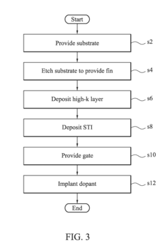
01 FinFET structure optimization for high-frequency performance
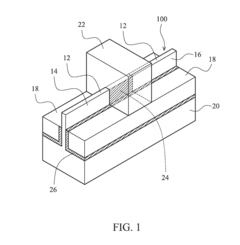
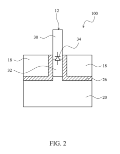
Optimizing the physical structure of FinFETs is crucial for high-frequency operations. This includes designing fin dimensions (height, width, and pitch), gate length scaling, and multi-fin configurations to reduce parasitic capacitance and resistance. These structural optimizations help improve the transistor's cutoff frequency, maximum oscillation frequency, and overall RF performance while maintaining good electrostatic control.- FinFET structure optimization for high-frequency performance: Optimizing the physical structure of FinFETs is crucial for high-frequency operations. This includes designing fin dimensions (height, width, and pitch), gate length scaling, and multi-fin configurations that minimize parasitic capacitance while maintaining current drive capability. These structural optimizations help reduce gate delay and improve cutoff frequencies, making FinFETs suitable for RF and high-frequency applications.
- Advanced gate engineering techniques: Gate engineering is essential for enhancing high-frequency performance in FinFETs. Techniques include using high-k dielectric materials, metal gate electrodes with optimized work functions, and gate-all-around configurations. These approaches reduce gate resistance, minimize short channel effects, and improve transconductance, resulting in better frequency response and switching speeds for high-frequency applications.
- Source/drain and contact optimization: Optimizing source/drain regions and contacts is critical for high-frequency FinFET operation. This involves implementing epitaxial source/drain regions with controlled doping profiles, reducing contact resistance through silicidation processes, and minimizing parasitic resistances in interconnects. These optimizations reduce RC delays and improve signal integrity at high frequencies.
- Circuit design techniques for high-frequency applications: Specialized circuit design techniques are employed to maximize FinFET performance in high-frequency applications. These include RF-optimized layout strategies, impedance matching networks, and noise reduction techniques. Advanced simulation models specifically calibrated for FinFET high-frequency behavior help designers predict and optimize circuit performance in applications such as 5G communications, radar systems, and high-speed data converters.
- Novel materials and integration schemes: Incorporating novel materials and integration schemes enhances FinFET high-frequency performance. This includes using strain engineering with SiGe or III-V materials to improve carrier mobility, implementing SOI substrates to reduce substrate coupling effects, and developing advanced interconnect materials with lower resistivity. These innovations help overcome traditional silicon limitations and push the frequency boundaries of FinFET technology.
02 Advanced gate engineering techniques
Gate engineering plays a significant role in enhancing FinFET high-frequency performance. Techniques include using high-k metal gate materials, gate-all-around structures, and optimized gate stack configurations. These approaches reduce gate resistance, minimize short channel effects, and improve transconductance, which are essential for high-frequency applications requiring fast switching speeds and high gain.Expand Specific Solutions03 Source/drain engineering for reduced parasitic effects
Engineering the source and drain regions is essential for high-frequency FinFET operation. This includes implementing epitaxial raised source/drain structures, optimized doping profiles, and advanced contact schemes to reduce parasitic resistance and capacitance. These techniques improve current drive capability and switching speed, which directly impact the high-frequency performance metrics of FinFET devices.Expand Specific Solutions04 Circuit design techniques for FinFET RF applications
Specialized circuit design techniques are employed to maximize FinFET performance in high-frequency applications. These include RF-optimized layout strategies, impedance matching networks, and noise reduction techniques. Advanced simulation models specifically developed for FinFET RF behavior help designers predict and optimize high-frequency performance parameters such as noise figure, linearity, and power efficiency.Expand Specific Solutions05 Novel materials and integration schemes
Incorporating novel materials and integration schemes enhances FinFET high-frequency capabilities. This includes using strain engineering, III-V channel materials, and advanced interconnect technologies. These innovations improve carrier mobility, reduce signal propagation delay, and enhance overall high-frequency performance while addressing challenges related to power consumption and thermal management in high-speed applications.Expand Specific Solutions
Key Industry Players in High-Frequency FinFET Development
The FinFET high-frequency validation market is currently in a growth phase, with increasing demand driven by 5G, IoT, and high-performance computing applications. The competitive landscape features established semiconductor giants like TSMC, Samsung, and IBM leading technological innovation, while foundries such as GlobalFoundries and SMIC are expanding capabilities to meet market demands. Companies including Qualcomm and NXP focus on specialized high-frequency applications, while equipment providers like Applied Materials develop advanced validation tools. Research institutions including the Institute of Microelectronics of Chinese Academy of Sciences and Shanghai Integrated Circuit Research & Development Center contribute significantly to technological advancement. The market is characterized by intense competition between established Western semiconductor companies and rapidly advancing Chinese manufacturers, with collaboration between industry and research institutions accelerating innovation in FinFET high-frequency validation methodologies.
International Business Machines Corp.
Technical Solution: IBM has pioneered advanced FinFET validation techniques for high-frequency operations through their silicon-on-insulator (SOI) technology platform. Their approach combines cryogenic testing methodologies with room-temperature characterization to develop comprehensive models that accurately predict performance across frequency ranges. IBM employs specialized RF test structures with calibrated de-embedding techniques to extract intrinsic device parameters at frequencies exceeding 100GHz. Their validation methodology incorporates quantum-mechanical simulations that account for carrier transport phenomena unique to nanoscale FinFET structures. IBM has developed proprietary compact models specifically calibrated for high-frequency operation that account for self-heating effects, substrate coupling, and layout-dependent parasitics. Their validation process includes reliability assessment under RF stress conditions to ensure performance consistency throughout device lifetime.
Strengths: Industry-leading research capabilities with strong academic partnerships; extensive experience with SOI technology which offers advantages for RF performance; sophisticated modeling capabilities that incorporate quantum effects. Weaknesses: Less manufacturing scale compared to pure-play foundries; validation methodologies may be more research-oriented than production-focused; higher cost structure.
GLOBALFOUNDRIES, Inc.
Technical Solution: GlobalFoundries has developed a specialized FinFET validation platform for high-frequency applications, particularly focused on their 22FDX and 12LP+ technology nodes. Their methodology employs a combination of on-wafer RF measurements and advanced electromagnetic simulations to characterize device performance up to millimeter-wave frequencies. GlobalFoundries utilizes custom-designed test structures with optimized ground-signal-ground (GSG) probe pads to minimize measurement parasitics. Their validation approach includes comprehensive characterization of noise parameters, which is critical for high-frequency analog and RF applications. GlobalFoundries has implemented automated test methodologies that enable statistical analysis across process corners to ensure robust high-frequency performance. Their platform incorporates specialized extraction techniques for parasitic elements that become dominant at high frequencies, with particular attention to substrate coupling effects that can degrade RF performance.
Strengths: Specialized focus on RF and mixed-signal applications; strong FD-SOI technology offering advantages for high-frequency operation; comprehensive design enablement ecosystem for RF applications. Weaknesses: Smaller manufacturing scale compared to TSMC and Samsung; less advanced process nodes may limit ultimate high-frequency performance; more limited resources for validation methodology development.
Critical Patents and Research in FinFET High-Frequency Validation
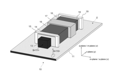
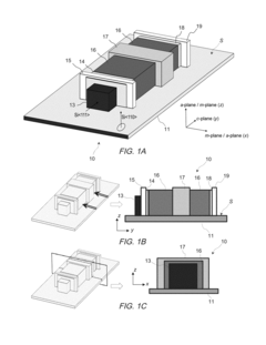
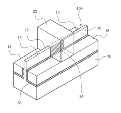
Non-polar, III-nitride semiconductor fin field-effect transistor
PatentInactiveUS9978872B1
Innovation
- A non-polar III-Nitride semiconductor finFET is developed with a fin grown along the c-direction on a Si(110) substrate, featuring sidewalls parallel to m and a planes, and a step profile to enhance turn-off/turn-on behavior, utilizing a dielectric layer and barrier material to prevent gate leakage, and doped III-Nitride material for contacts.

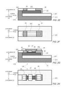
Fin field effect transistor (finfet)
PatentActiveUS20150200302A1
Innovation
- Incorporating a high-k dielectric material adjacent to the fin to redistribute the potential drop more evenly across the diode junction, reducing the local electric field strength and thereby minimizing band-to-band tunneling without requiring a reduction in doping levels, thus addressing the trade-off between punch-through and band-to-band tunneling.
Thermal Management Considerations for High-Frequency Operations
Thermal management has emerged as a critical factor in the validation of FinFET devices for high-frequency operations. As operational frequencies increase, power density within these nanoscale transistors rises dramatically, creating significant thermal challenges that can compromise both performance and reliability. The self-heating effect in FinFETs is particularly pronounced due to their three-dimensional structure and reduced thermal conductivity pathways compared to planar transistors.
When validating FinFETs for high-frequency applications, engineers must implement comprehensive thermal monitoring systems capable of detecting temperature variations at the nanoscale level. Advanced infrared thermography and scanning thermal microscopy techniques have proven effective for capturing real-time thermal profiles during high-frequency switching. These measurements must be correlated with electrical performance parameters to establish reliable thermal-electrical models.
The development of accurate electrothermal simulation frameworks represents another crucial aspect of thermal management validation. These frameworks must account for the complex geometry of FinFET structures and incorporate temperature-dependent material properties. Recent advancements in multi-physics simulation tools have enabled more precise prediction of hotspot formation and thermal gradients across the device under various operational conditions.
Heat dissipation strategies must be evaluated as part of the validation process. Novel packaging solutions incorporating advanced thermal interface materials have demonstrated significant improvements in heat extraction efficiency. The integration of localized cooling mechanisms, such as microfluidic channels and phase-change materials, shows promise for managing thermal loads in high-density FinFET arrays operating at elevated frequencies.
Reliability testing under thermal stress conditions constitutes an essential component of the validation methodology. Accelerated life testing protocols must be designed to simulate the thermal cycling experienced during high-frequency operation. Statistical analysis of failure modes related to thermal effects helps establish operational boundaries and safety margins for different application scenarios.
The impact of process variations on thermal behavior requires careful assessment during validation. Manufacturing tolerances can significantly affect thermal conductivity pathways and heat generation profiles. Comprehensive characterization across multiple process corners enables the development of robust design guidelines that account for thermal variability in high-frequency applications.
Ultimately, successful thermal management validation for high-frequency FinFET operation requires an integrated approach combining advanced measurement techniques, sophisticated modeling frameworks, and innovative cooling solutions. The validation methodology must evolve continuously to address emerging thermal challenges as FinFET technology scales to smaller dimensions and higher operational frequencies.
Reliability and Aging Effects Assessment Framework
Reliability and aging effects represent critical challenges for FinFET devices operating at high frequencies. A comprehensive assessment framework must be established to validate these devices under various stress conditions and predict their long-term performance. The framework should incorporate multiple testing methodologies that specifically target high-frequency degradation mechanisms, which differ significantly from those observed in standard DC operations.
The assessment framework begins with accelerated aging tests under various bias and temperature conditions while monitoring high-frequency parameters. Hot carrier injection (HCI), bias temperature instability (BTI), and time-dependent dielectric breakdown (TDDB) tests must be adapted to include RF performance metrics such as transconductance, cutoff frequency, and noise figure. These tests should be conducted at frequencies matching the intended application range, typically 10-100 GHz for advanced FinFET nodes.
Statistical analysis forms a crucial component of the framework, as device-to-device variations become more pronounced at high frequencies. Monte Carlo simulations incorporating process variations should be integrated with aging models to predict performance distribution shifts over time. This approach enables more accurate lifetime predictions than traditional single-device characterization methods.
The framework must also include specialized RF reliability monitors and on-chip sensors capable of in-situ measurements during high-frequency operation. Ring oscillators modified for RF operation, RF SRAM cells, and transmission line test structures provide valuable data on how aging affects actual circuit performance rather than just device parameters. These structures should be designed to isolate specific degradation mechanisms while maintaining relevance to practical applications.
Correlation between DC and RF aging characteristics represents another essential element of the framework. Establishing mathematical relationships between easily measured DC parameters and critical RF metrics enables more efficient testing protocols and better predictive models. Recent research indicates that while some degradation mechanisms affect both domains similarly, others show frequency-dependent behavior that requires specific modeling approaches.
Finally, the framework should incorporate feedback mechanisms to refine compact models based on measured aging data. Physics-based aging models must be calibrated against experimental results and continuously updated to improve prediction accuracy. This closed-loop approach ensures that design tools can accurately account for reliability effects when simulating high-frequency circuits using FinFET technology, ultimately enabling robust designs with realistic performance margins over the intended product lifetime.
Unlock deeper insights with Patsnap Eureka Quick Research — get a full tech report to explore trends and direct your research. Try now!
Generate Your Research Report Instantly with AI Agent
Supercharge your innovation with Patsnap Eureka AI Agent Platform!