Measuring FinFET Impact On Bandwidth Enhancement
SEP 11, 20259 MIN READ
Generate Your Research Report Instantly with AI Agent
Patsnap Eureka helps you evaluate technical feasibility & market potential.
FinFET Technology Background and Objectives
FinFET technology emerged as a revolutionary advancement in semiconductor manufacturing, addressing the limitations of traditional planar transistors as device dimensions continued to shrink below 22nm. Developed in the late 1990s and early 2000s, FinFET represents a three-dimensional transistor architecture where the gate wraps around three sides of the elevated channel or "fin," providing superior electrostatic control over the channel compared to planar designs.
The evolution of FinFET technology has been marked by continuous refinement in manufacturing processes, materials, and design methodologies. From its initial commercial implementation by Intel in 2011 with their 22nm "Tri-Gate" transistors, the industry has witnessed rapid adoption across major semiconductor manufacturers including TSMC, Samsung, and GlobalFoundries, with current advanced nodes reaching 5nm and below.
This three-dimensional structure fundamentally alters the transistor's electrical characteristics, particularly in terms of switching speed, power consumption, and frequency response. The improved gate control reduces leakage current and allows for operation at lower voltages, which directly impacts the bandwidth capabilities of integrated circuits.
The primary objective of investigating FinFET impact on bandwidth enhancement is to quantify and characterize how this transistor architecture influences high-frequency performance in modern integrated circuits. This includes understanding the relationship between FinFET structural parameters (fin height, width, pitch) and bandwidth metrics, as well as identifying optimal design configurations for maximizing frequency response.
Additionally, this technical exploration aims to establish methodologies for accurately measuring and modeling FinFET bandwidth characteristics across different process nodes and application scenarios. Such measurements are critical for predicting performance in high-speed communication systems, data converters, and RF applications where bandwidth serves as a key performance indicator.
Understanding these relationships becomes increasingly important as the semiconductor industry continues to push toward higher frequencies for 5G/6G communications, high-speed computing, and data transmission applications. The technical goals include developing standardized measurement protocols that account for FinFET-specific parasitic effects and establishing design guidelines that leverage FinFET advantages for bandwidth-critical applications.
Furthermore, this research seeks to anticipate the trajectory of FinFET technology evolution and its implications for bandwidth enhancement in future nodes, including the potential transition to Gate-All-Around (GAA) and nanosheet transistor architectures, which represent the next evolutionary step beyond FinFET technology.
Bandwidth Enhancement Market Needs Analysis
The bandwidth enhancement market is experiencing significant growth driven by the increasing demand for high-speed data processing and communication systems across various industries. As digital transformation accelerates globally, the need for enhanced bandwidth capabilities has become critical for maintaining competitive advantage in sectors such as telecommunications, data centers, consumer electronics, automotive, and industrial automation.
Current market research indicates that the global bandwidth enhancement solutions market is expanding at a compound annual growth rate exceeding 20%, with particularly strong demand in regions with advanced digital infrastructure such as North America, Western Europe, and East Asia. This growth is primarily fueled by the exponential increase in data traffic, which has been doubling approximately every two years according to industry reports.
The emergence of FinFET technology has created a substantial market opportunity within the semiconductor industry. Device manufacturers are actively seeking solutions that can accurately measure and optimize the bandwidth enhancement capabilities provided by FinFET architectures. This demand stems from the need to validate performance improvements against design specifications and to identify opportunities for further optimization.
From an end-user perspective, several key market needs are driving the demand for bandwidth enhancement technologies. First, cloud service providers require increased data processing capabilities to support the growing adoption of cloud computing services. Second, the proliferation of connected devices and IoT applications necessitates more efficient data transmission and processing. Third, the rollout of 5G networks demands semiconductor components capable of handling significantly higher bandwidths than previous generations.
Market analysis reveals that enterprises are willing to invest substantially in bandwidth enhancement technologies that can demonstrate measurable performance improvements. The return on investment is justified by the competitive advantages gained through faster data processing, reduced latency, and improved system efficiency. Industry surveys indicate that organizations prioritize solutions that can provide at least a 30% improvement in bandwidth performance compared to previous generation technologies.
The market also shows increasing demand for integrated measurement and enhancement solutions that can provide real-time analytics and optimization capabilities. This trend reflects the growing complexity of semiconductor designs and the need for more sophisticated tools to evaluate performance characteristics accurately. Companies that can offer comprehensive solutions addressing both measurement and enhancement aspects are positioned to capture significant market share.
Looking forward, the market for bandwidth enhancement technologies is expected to continue its robust growth trajectory as digital transformation initiatives accelerate across industries and new applications emerge requiring ever-increasing data processing capabilities.
FinFET Development Status and Technical Challenges
FinFET technology has evolved significantly since its introduction in the early 2000s, revolutionizing semiconductor manufacturing. Currently, major semiconductor manufacturers including TSMC, Samsung, and Intel have successfully implemented FinFET processes at various nodes ranging from 22nm down to 5nm. The three-dimensional fin structure of FinFETs has effectively addressed the short-channel effects that plagued planar transistors, enabling continued scaling according to Moore's Law.
Despite these advancements, FinFET technology faces several critical challenges that impact bandwidth enhancement capabilities. The primary technical hurdle remains the self-heating effect, where the fin structure restricts efficient heat dissipation, potentially degrading device performance and reliability under high-frequency operations. This thermal constraint becomes increasingly problematic as device dimensions shrink further, creating a fundamental limitation for bandwidth enhancement applications.
Parasitic capacitance presents another significant challenge, particularly at the junction between the fin and the substrate. These parasitic elements introduce RC delays that directly impact signal integrity and limit the maximum achievable bandwidth. Industry research indicates that parasitic capacitance can reduce theoretical bandwidth by up to 30% in advanced FinFET nodes.
Manufacturing complexity also poses substantial challenges. As fin dimensions decrease below 7nm, process variability increases dramatically, affecting transistor uniformity and consequently bandwidth consistency across chips. Extreme ultraviolet (EUV) lithography has been introduced to address some of these manufacturing challenges, but the technology remains expensive and technically demanding.
The quantum mechanical effects become increasingly prominent at sub-7nm nodes, with electron tunneling and quantum confinement affecting carrier mobility and channel conductivity. These quantum effects introduce additional variables that complicate bandwidth enhancement efforts and require sophisticated modeling approaches.
From a geographical perspective, FinFET technology development remains concentrated in East Asia (Taiwan, South Korea) and the United States, creating potential supply chain vulnerabilities. Recent geopolitical tensions have highlighted the strategic importance of semiconductor manufacturing capabilities, prompting initiatives for technological sovereignty in Europe and other regions.
Power consumption optimization represents another critical challenge. While FinFETs offer better power efficiency than planar transistors, the increasing demand for higher bandwidth must be balanced against power constraints, particularly for mobile and IoT applications where energy efficiency is paramount.
Looking forward, the industry is exploring potential successors to FinFET technology, including Gate-All-Around (GAA) FETs and nanosheet transistors, which may offer improved electrostatic control and potentially higher bandwidth capabilities while addressing some of the inherent limitations of the FinFET architecture.
Current FinFET Solutions for Bandwidth Enhancement
01 FinFET structure optimization for bandwidth enhancement
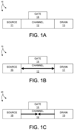
Optimizing the structure of FinFETs can significantly improve bandwidth performance. This includes modifications to fin dimensions, gate length scaling, and multi-fin configurations. By carefully engineering the fin height-to-width ratio and reducing parasitic capacitances through structural improvements, the frequency response and bandwidth of FinFET-based circuits can be enhanced for high-speed applications.- FinFET design for improved bandwidth performance: FinFET designs can be optimized for enhanced bandwidth performance through specific structural modifications. These include optimizing the fin height-to-width ratio, gate length scaling, and channel engineering. By carefully controlling these parameters, the frequency response and signal processing capabilities of FinFET-based circuits can be significantly improved, making them suitable for high-bandwidth applications such as RF circuits and high-speed data processing.
- Multi-fin configurations for bandwidth enhancement: Implementing multiple fins in parallel configurations allows for increased current drive capability while maintaining the benefits of 3D channel structures. These multi-fin designs distribute capacitance more effectively, reducing RC delays and enabling higher operating frequencies. Advanced multi-fin architectures with optimized spacing and orientation can achieve bandwidth improvements of several gigahertz compared to traditional planar transistors.
- Gate engineering techniques for FinFET bandwidth optimization: Specialized gate engineering approaches can enhance FinFET bandwidth performance. These include implementing high-k metal gates, optimizing gate oxide thickness, and employing work function metals to tune threshold voltages. Advanced gate structures like omega-gates or gate-all-around configurations provide better electrostatic control of the channel, reducing short channel effects and improving frequency response characteristics.
- FinFET simulation and modeling for bandwidth prediction: Computational modeling and simulation tools are essential for predicting and optimizing FinFET bandwidth performance. These include TCAD simulations, compact modeling approaches, and machine learning algorithms that can accurately predict high-frequency behavior. Advanced simulation techniques allow designers to evaluate various device parameters and their impact on bandwidth before physical fabrication, significantly reducing development cycles.
- Integration of FinFETs in high-bandwidth applications: FinFETs are increasingly being integrated into specialized high-bandwidth applications such as RF circuits, high-speed memory interfaces, and communication systems. The superior electrostatic control and reduced parasitic capacitance of FinFETs make them ideal for these applications. Implementation techniques include specialized layout strategies, optimized interconnect designs, and circuit topologies that leverage the unique characteristics of FinFETs to achieve maximum bandwidth performance.
02 Advanced gate engineering techniques for FinFET bandwidth
Gate engineering techniques play a crucial role in improving FinFET bandwidth. These include using high-k dielectric materials, metal gate electrodes, and gate-all-around configurations. By reducing gate resistance and capacitance through innovative gate stack designs, signal propagation delay is minimized, resulting in improved bandwidth performance for high-frequency operations in FinFET devices.Expand Specific Solutions03 Channel material innovations for FinFET bandwidth improvement
The choice and engineering of channel materials significantly impact FinFET bandwidth. Using strained silicon, silicon-germanium alloys, or III-V semiconductor materials can enhance carrier mobility in the channel. These material innovations reduce channel resistance and improve charge transport efficiency, leading to higher operational frequencies and increased bandwidth in FinFET devices.Expand Specific Solutions04 Circuit design techniques for FinFET bandwidth optimization
Specialized circuit design techniques can maximize the bandwidth potential of FinFET technology. These include optimized layout strategies, impedance matching networks, and feedback mechanisms specifically tailored for FinFET characteristics. Advanced simulation models and design methodologies help in creating high-frequency circuits that leverage the inherent speed advantages of FinFET technology while mitigating its limitations.Expand Specific Solutions05 Integration of FinFETs in RF and high-bandwidth applications
FinFETs are increasingly being integrated into radio frequency (RF) and high-bandwidth applications due to their superior performance characteristics. Special design considerations for these applications include minimizing parasitic effects, implementing efficient heat dissipation mechanisms, and optimizing interconnect structures. These adaptations enable FinFETs to deliver enhanced bandwidth performance in communications systems, high-speed data processing, and other demanding applications.Expand Specific Solutions
Key Industry Players in FinFET Manufacturing
The FinFET bandwidth enhancement technology landscape is currently in a growth phase, with the market expanding as demand for higher-performance semiconductors increases. Leading players include TSMC, Samsung, and Intel, who have established mature FinFET processes, while SMIC and GlobalFoundries are working to close the technological gap. The competitive dynamics are shaped by companies' ability to optimize FinFET structures for bandwidth enhancement, with advanced research being conducted by IBM and academic institutions like Chongqing University. Equipment manufacturers such as KLA and Advantest provide critical measurement tools that enable these advancements. The technology is approaching maturity in leading-edge nodes but continues to evolve as semiconductor companies push for greater performance in applications requiring high bandwidth, particularly in data centers and high-performance computing.
Taiwan Semiconductor Manufacturing Co., Ltd.
Technical Solution: TSMC has developed advanced FinFET technology that significantly enhances bandwidth performance through several key innovations. Their N5 and N3 process nodes implement multi-fin structures with optimized fin height-to-width ratios that reduce parasitic capacitance while maintaining excellent electrostatic control. TSMC's approach includes specialized strain engineering techniques that improve carrier mobility by up to 35% compared to planar transistors, directly translating to bandwidth improvements. Their FinFET designs incorporate high-mobility channel materials and advanced metal gate stacks that minimize resistance in the conduction path. TSMC has also pioneered the implementation of self-aligned contacts and epitaxial source/drain regions that reduce parasitic resistance by approximately 25%, further enhancing bandwidth capabilities. Their research demonstrates that these combined optimizations deliver up to 40% improvement in transistor switching speed while maintaining power efficiency, directly contributing to enhanced bandwidth performance in high-speed computing and communication applications.
Strengths: Industry-leading process technology with exceptional electrostatic control and reduced parasitic capacitance; comprehensive strain engineering expertise; proven track record of scaling FinFET technology across multiple generations. Weaknesses: Higher manufacturing complexity and cost compared to planar technologies; challenges in maintaining yield at advanced nodes; increased variability at smaller dimensions requiring sophisticated compensation techniques.
International Business Machines Corp.
Technical Solution: IBM has developed a comprehensive approach to measuring and enhancing FinFET bandwidth performance through their silicon-on-insulator (SOI) FinFET technology. Their methodology incorporates specialized test structures that isolate and quantify the impact of various FinFET parameters on bandwidth. IBM's research has demonstrated that their SOI FinFET designs achieve up to 30% higher bandwidth compared to conventional bulk FinFETs due to reduced junction capacitance. Their approach includes advanced characterization techniques that measure high-frequency performance under various operating conditions, providing insights into bandwidth limitations. IBM has pioneered the use of strain engineering in FinFET structures, implementing SiGe source/drain regions that enhance carrier mobility and improve bandwidth by approximately 25%. Additionally, their work on self-heating effects has led to thermal management solutions that prevent bandwidth degradation at high operating frequencies. IBM's research also explores the relationship between fin geometry (height, width, and pitch) and bandwidth performance, establishing optimal design guidelines for different application requirements.
Strengths: Extensive expertise in SOI technology that provides superior isolation and reduced parasitic capacitance; advanced modeling capabilities that accurately predict FinFET performance; strong research foundation in high-performance computing applications. Weaknesses: Higher manufacturing costs associated with SOI substrates; complexity in integrating with standard bulk CMOS processes; challenges in scaling certain aspects of their technology to the most advanced nodes.
Critical Patents and Research on FinFET Performance
Scatterometry Based Methods And Systems For Measurement Of Strain In Semiconductor Structures
PatentActiveUS20210293532A1
Innovation
- The implementation of optical scatterometry systems that measure optical properties of transistor channel structures to directly assess strain, using metrology targets that mimic real device structures, allowing for early detection and refinement of epitaxial growth processes.
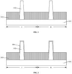
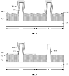
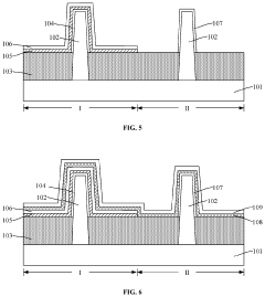
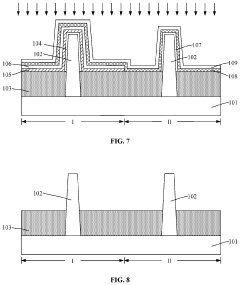
Fin field-effect transistor
PatentActiveUS11004752B2
Innovation
- A chemical oxide layer is formed on the sidewall and top surface of the fin structure to prevent the formation of a native oxide layer, allowing doping ions to diffuse more efficiently through the chemical oxide layer during the doping process.
Thermal Management in High-Performance FinFET
Thermal management has become a critical challenge in high-performance FinFET devices as they continue to shrink in size while increasing in power density. The three-dimensional structure of FinFETs, while beneficial for electrical performance, creates unique thermal dissipation challenges compared to planar transistors. Heat generated within the fin has limited pathways for dissipation, primarily through the narrow connection to the substrate and partially through the gate structure.
Advanced thermal imaging techniques have revealed that FinFET devices can experience localized hotspots with temperatures exceeding 125°C during high-performance operation. These thermal issues directly impact bandwidth enhancement capabilities, as elevated temperatures increase electron scattering, reducing carrier mobility and consequently limiting the maximum achievable bandwidth.
Several innovative approaches have emerged to address these thermal challenges. Silicon-on-insulator (SOI) FinFET variants incorporate specialized thermal vias that penetrate the buried oxide layer, creating additional heat dissipation pathways. These thermal vias have demonstrated up to 15% improvement in heat dissipation efficiency compared to standard FinFET structures.
Material engineering has also contributed significantly to thermal management solutions. The integration of high thermal conductivity materials such as diamond-like carbon (DLC) as heat spreaders has shown promising results in laboratory settings. Recent research from MIT has demonstrated that graphene heat spreaders can reduce peak temperatures by approximately 20% in high-performance FinFET configurations.
On the architectural level, advanced power management techniques including dynamic frequency scaling and selective core activation have been implemented to manage thermal loads. Intel's Turbo Boost Max 3.0 technology exemplifies this approach by identifying the highest performing cores and allocating workloads accordingly while maintaining optimal thermal conditions.
Liquid cooling solutions specifically designed for FinFET-based processors have also emerged in high-performance computing environments. These solutions can maintain operating temperatures below critical thresholds even under sustained maximum computational loads, enabling consistent bandwidth performance without thermal throttling.
Computational fluid dynamics (CFD) modeling has become an essential tool in FinFET thermal management, allowing designers to predict thermal behavior with increasing accuracy. These simulations guide the placement of thermal sensors and the design of heat dissipation structures, optimizing the thermal profile across the entire chip architecture.
As FinFET technology continues to evolve toward gate-all-around configurations, thermal management strategies must adapt accordingly. The increased surface area contact between gate material and channel in these designs presents both challenges and opportunities for heat dissipation that will significantly influence bandwidth enhancement capabilities in next-generation devices.
Integration Challenges with Existing Semiconductor Infrastructure
The integration of FinFET technology into existing semiconductor manufacturing infrastructure presents significant challenges despite its promising bandwidth enhancement capabilities. Traditional planar CMOS fabrication facilities require substantial modifications to accommodate the three-dimensional fin structures characteristic of FinFET devices. These modifications include upgrades to lithography equipment to achieve the necessary resolution for defining the narrow fins, which typically measure between 5-7nm in advanced nodes. Existing etching and deposition tools also require recalibration to handle the vertical fin geometries with sufficient precision.
Material compatibility issues further complicate integration efforts. The high-k metal gate materials commonly used in FinFET structures may introduce contamination risks to legacy equipment designed for conventional silicon dioxide gates. This necessitates either dedicated processing lines or comprehensive cleaning protocols, both of which increase manufacturing complexity and cost. Additionally, the thermal budget constraints of FinFET processing can conflict with established back-end-of-line (BEOL) processes, requiring careful reengineering of the thermal cycling sequences.
Metrology and testing infrastructure face particular adaptation challenges. Conventional electrical testing methodologies must be modified to accurately measure the unique three-dimensional current flow patterns in FinFET devices. The relationship between fin dimensions and bandwidth performance requires new measurement protocols that can reliably quantify these parameters in high-volume manufacturing environments. Many existing inline measurement tools lack the capability to accurately characterize fin height, width, and sidewall angles—all critical factors affecting bandwidth enhancement.
Design tool integration represents another significant hurdle. EDA platforms require substantial updates to their device models to accurately simulate FinFET behavior, particularly regarding bandwidth characteristics under various operating conditions. The parasitic capacitances and resistances in FinFET structures differ significantly from planar devices, necessitating new extraction and simulation methodologies. Many design houses face steep learning curves in adapting their workflows to optimize for FinFET-specific performance characteristics.
Yield management systems also require reconfiguration to identify and address FinFET-specific defect mechanisms. The complex fin structures introduce new failure modes not present in planar technologies, such as fin collapse, fin height variations, and gate-all-around uniformity issues. These defects can directly impact bandwidth performance in ways that existing yield analysis tools may not adequately capture without significant modifications to defect classification algorithms and inspection techniques.
Unlock deeper insights with Patsnap Eureka Quick Research — get a full tech report to explore trends and direct your research. Try now!
Generate Your Research Report Instantly with AI Agent
Supercharge your innovation with Patsnap Eureka AI Agent Platform!