

Exploring FinFET Layout Optimization For Space Constraints
SEP 11, 202510 MIN READ
Generate Your Research Report Instantly with AI Agent
PatSnap Eureka helps you evaluate technical feasibility & market potential.
FinFET Technology Evolution and Objectives
FinFET technology emerged as a revolutionary advancement in semiconductor manufacturing, addressing the limitations of traditional planar transistors as device dimensions continued to shrink below 22nm. Since its commercial introduction in 2011, FinFET has evolved through multiple generations, each bringing significant improvements in performance, power efficiency, and density. The three-dimensional fin structure allows for better electrostatic control of the channel, substantially reducing leakage current and enabling further scaling of transistor dimensions.
The evolution of FinFET technology can be traced through several key milestones. Initially, single-fin designs dominated, but as technology matured, multi-fin configurations became standard to increase drive current capabilities. Gate pitch and fin pitch have consistently decreased across generations, from approximately 90nm and 60nm respectively in early implementations to below 40nm and 30nm in current advanced nodes. This scaling trajectory has enabled the semiconductor industry to maintain its adherence to Moore's Law despite the physical limitations encountered with planar transistors.
Space constraints represent one of the most significant challenges in modern FinFET implementation. As device dimensions continue to shrink, the layout optimization becomes increasingly critical to balance performance requirements with area efficiency. The primary objective in FinFET layout optimization is to maximize transistor density while maintaining electrical performance characteristics and ensuring manufacturability. This involves careful consideration of fin spacing, gate placement, and contact arrangements to minimize the overall footprint.
Current research objectives in FinFET technology focus on overcoming several key limitations. These include reducing variability in fin dimensions, which directly impacts threshold voltage consistency; minimizing parasitic capacitance between closely packed structures; and developing novel layout techniques that can accommodate the increasing complexity of circuit designs while maintaining yield. Additionally, there is significant interest in exploring new materials and structural modifications to extend FinFET scalability beyond current limitations.
The industry is also witnessing a transition toward alternative architectures such as Gate-All-Around (GAA) FETs and nanosheet transistors, which represent the natural evolution of FinFET technology. However, for many applications, optimized FinFET designs remain the most cost-effective solution, driving continued research into layout optimization techniques specifically addressing space constraints. These optimization efforts aim to extract maximum performance from existing manufacturing processes while preparing for the eventual transition to next-generation transistor architectures.
Market Demand for Space-Efficient FinFET Solutions
The semiconductor industry is witnessing an unprecedented demand for space-efficient FinFET solutions, driven primarily by the continuous miniaturization of electronic devices and the increasing complexity of integrated circuits. Market research indicates that the global FinFET technology market is experiencing robust growth, with particular emphasis on applications requiring optimal performance within strict spatial constraints.
Consumer electronics manufacturers represent a significant market segment demanding space-efficient FinFET solutions. As smartphones, tablets, and wearable devices continue to incorporate more functionality while maintaining or reducing form factors, chip designers face mounting pressure to optimize transistor layouts. This trend is particularly evident in premium mobile devices where manufacturers compete on both performance and device thinness.
Data center operators constitute another major market driver, as they seek to maximize computational density while minimizing power consumption and heat generation. The economics of data center operation increasingly favor chips that can deliver more processing power per unit volume, creating substantial demand for spatially optimized FinFET designs that maintain performance integrity.
Automotive electronics represent an emerging but rapidly growing market segment. Advanced driver-assistance systems (ADAS) and autonomous driving technologies require sophisticated processing capabilities in environments with severe space limitations. These applications demand FinFET solutions that can withstand harsh operating conditions while fitting into constrained vehicle architectures.
Market analysis reveals that aerospace and defense applications are also creating specialized demand for space-efficient FinFET technology. Satellite systems, avionics, and military electronics all operate under extreme space and weight constraints while requiring exceptional reliability and performance.
The Internet of Things (IoT) ecosystem is driving demand for ultra-compact, energy-efficient processors that can be embedded in a vast array of connected devices. This market segment values FinFET designs that minimize silicon area without compromising on power efficiency or computational capability.
Industry forecasts suggest that manufacturers who can deliver FinFET solutions with optimal space utilization will capture significant market share across these segments. The economic value proposition is compelling: space-efficient designs typically translate to higher yields per wafer, reduced packaging costs, and improved thermal management characteristics.
Regional market analysis indicates particularly strong demand growth in Asia-Pacific semiconductor manufacturing hubs, where intense competition drives innovation in layout optimization techniques. North American markets show strong demand from cloud service providers and defense contractors, while European demand centers on automotive and industrial applications requiring space-efficient solutions.
Current FinFET Layout Challenges in Constrained Environments
As FinFET technology continues to evolve and scale down to increasingly smaller nodes, layout engineers face significant challenges in optimizing designs within constrained environments. The primary challenge stems from the three-dimensional nature of FinFET structures, which introduces complex design considerations not present in traditional planar MOSFET technologies. In space-constrained applications such as mobile SoCs, IoT devices, and automotive microcontrollers, these challenges become particularly acute.
The fin geometry itself presents a fundamental layout constraint. Unlike planar technologies where transistor width can be continuously adjusted, FinFET width is quantized in multiples of individual fins. This quantization limits design flexibility, especially in analog circuits where precise transistor sizing is critical. Engineers must develop innovative layout techniques to achieve the desired electrical characteristics while adhering to these quantization constraints.
Contact and via placement represents another significant challenge in constrained FinFET layouts. The reduced pitch between fins limits the available space for contacts, often requiring complex routing solutions. In densely packed layouts, this can lead to increased parasitic resistance and capacitance, degrading circuit performance. Advanced contact schemes such as buried power rails and backside power delivery are being explored to address these limitations.
Self-heating effects become more pronounced in tightly packed FinFET layouts. The fin structure restricts heat dissipation pathways, potentially leading to thermal hotspots that can impact device reliability and performance. This is particularly problematic in high-performance computing applications where thermal management is already challenging. Layout engineers must carefully consider thermal gradients and implement appropriate spacing and cooling strategies.
Lithography constraints add another layer of complexity. As feature sizes approach the limits of current lithographic capabilities, design rules become increasingly restrictive. Multiple patterning techniques required for advanced nodes introduce complex layout dependencies and restrictions. These constraints often force compromises between optimal electrical performance and manufacturability.
Electrostatic integrity presents unique challenges in dense FinFET layouts. Closely packed fins can experience increased electrostatic coupling, leading to threshold voltage variations and other undesirable effects. Layout-dependent effects become more pronounced, requiring sophisticated modeling and simulation approaches to ensure reliable circuit operation.
Power distribution networks face significant constraints in dense FinFET designs. The limited metal resources in upper layers must be carefully allocated to minimize IR drop while maintaining signal integrity. This often requires complex power grid optimizations and sometimes necessitates architectural changes to accommodate power delivery requirements within space constraints.
Current Layout Optimization Techniques for FinFETs
01 Layout optimization techniques for FinFET devices
Various techniques can be employed to optimize the layout of FinFET devices, including fin placement strategies, gate positioning, and overall device arrangement. These optimization methods aim to improve performance metrics such as power consumption, speed, and area efficiency. Advanced algorithms and computational methods help designers achieve optimal layouts while maintaining design rule compliance and manufacturability.- Layout optimization techniques for FinFET devices: Various techniques can be employed to optimize the layout of FinFET devices, including fin placement strategies, gate positioning, and overall device geometry. These optimization methods aim to improve performance metrics such as power consumption, switching speed, and area efficiency. Advanced algorithms and computational methods help designers achieve optimal fin arrangements while maintaining design rule compliance and manufacturability.
- Design rule checking and verification for FinFET layouts: Design rule checking (DRC) and verification processes specific to FinFET technology ensure that layouts meet manufacturing requirements and performance specifications. These processes involve validating fin dimensions, spacing, alignment, and other critical parameters. Automated tools can identify potential issues early in the design process, reducing the need for costly redesigns and improving yield in production.
- Computational methods for FinFET layout optimization: Advanced computational methods and algorithms are used to optimize FinFET layouts, including machine learning approaches, genetic algorithms, and simulation-based optimization. These methods can efficiently explore the design space to find optimal solutions that balance multiple competing objectives such as performance, power, and area. Computational techniques enable designers to evaluate numerous layout configurations rapidly and identify the most promising candidates.
- Multi-fin arrangement and patterning strategies: Optimizing the arrangement and patterning of multiple fins in FinFET designs is crucial for achieving desired electrical characteristics. Strategies include varying fin height, width, and spacing to control current flow and reduce parasitic effects. Advanced patterning techniques help maintain uniformity across the device while maximizing performance. These approaches address challenges related to process variations and lithography limitations in advanced technology nodes.
- Integration of FinFET layout optimization in EDA workflows: Electronic Design Automation (EDA) workflows incorporate specialized tools and methodologies for FinFET layout optimization. These integrated approaches enable seamless optimization throughout the design process, from initial placement to final verification. EDA tools can automatically apply optimization techniques while considering manufacturing constraints, design rules, and performance targets. This integration streamlines the design process and helps achieve optimal results with reduced manual intervention.
02 Design rule checking and verification for FinFET layouts
Design rule checking (DRC) and verification processes specific to FinFET technology ensure that layouts meet manufacturing requirements and performance specifications. These processes involve validating fin dimensions, spacing, gate alignment, and other critical parameters. Automated tools can identify potential issues early in the design process, reducing the need for costly redesigns and improving yield rates.Expand Specific Solutions03 Multi-gate and 3D structure optimization for FinFETs
Optimization of multi-gate structures and three-dimensional aspects of FinFET designs is crucial for maximizing device performance. This includes optimizing fin height, width, and pitch, as well as gate length and positioning. Advanced simulation tools can model the electrical characteristics of these complex 3D structures, allowing designers to fine-tune parameters for specific application requirements.Expand Specific Solutions04 Computational methods for FinFET layout optimization
Computational approaches including machine learning algorithms, genetic algorithms, and other optimization techniques can be applied to FinFET layout design. These methods can efficiently explore the vast design space to identify optimal configurations that balance multiple competing objectives such as performance, power consumption, and area. Simulation-based optimization frameworks allow for rapid evaluation of different layout options.Expand Specific Solutions05 Integration of FinFET optimization with overall circuit design
Effective FinFET layout optimization must be integrated with higher-level circuit design considerations. This includes optimizing cell libraries specifically for FinFET technology, developing placement and routing strategies that leverage FinFET characteristics, and ensuring compatibility with existing design flows. Holistic approaches that consider both device-level and system-level optimization yield the best overall circuit performance.Expand Specific Solutions
Leading Semiconductor Companies in FinFET Development
The FinFET layout optimization market is currently in a growth phase, with increasing demand for space-efficient chip designs in compact electronic devices. The global market is estimated to reach $25 billion by 2025, driven by miniaturization trends in consumer electronics and automotive applications. Leading players include Taiwan Semiconductor Manufacturing Co. (TSMC), which dominates with advanced 5nm and 3nm FinFET processes, followed by Samsung Electronics with competitive 7nm technology. GLOBALFOUNDRIES and United Microelectronics Corp. (UMC) maintain significant market shares with specialized FinFET solutions. Chinese manufacturers like SMIC are rapidly advancing their capabilities but face technological gaps compared to industry leaders. IBM and Apple represent key research contributors and end-users respectively, pushing boundaries in layout optimization techniques for increasingly complex chip designs.
Taiwan Semiconductor Manufacturing Co., Ltd.
Technical Solution: TSMC has pioneered advanced FinFET layout optimization techniques for space-constrained applications through their N5 and N3 process nodes. Their approach involves implementing self-aligned double/quadruple patterning (SADP/SAQP) to achieve ultra-dense fin structures with pitches below 30nm. TSMC's solution incorporates continuous fin diffusion regions with optimized gate placement to maximize transistor density while maintaining performance. Their N3 technology specifically addresses space constraints by implementing a "track height reduction" methodology that decreases the standard cell height by approximately 20% compared to previous generations. TSMC has also developed specialized FinFET variants with variable fin heights and widths within the same die to optimize for different performance/power requirements in space-limited areas. Their EUV lithography integration enables more precise fin definition and placement, reducing edge placement errors to below 2nm, which is critical for maintaining consistent electrical characteristics in tightly packed layouts.
Strengths: Industry-leading process node advancement with proven high-volume manufacturing capability; superior EUV lithography implementation allowing for more precise fin placement; comprehensive design rule optimization tailored for different application domains. Weaknesses: Higher manufacturing costs compared to less advanced nodes; complex design rules that may limit layout flexibility for certain applications; requires sophisticated EDA tools to fully leverage layout optimization capabilities.
GLOBALFOUNDRIES, Inc.
Technical Solution: GLOBALFOUNDRIES has developed a specialized FinFET layout optimization approach called "22FDX-FinFET Hybrid" that addresses space constraints through strategic integration of planar and FinFET technologies. Their solution implements a variable fin height architecture that allows designers to optimize transistor footprint based on performance requirements in different circuit blocks. For extremely space-constrained applications, GLOBALFOUNDRIES employs a "fin depopulation" technique that selectively removes fins in non-critical paths to create room for routing and other components while maintaining overall circuit performance. Their 12nm FinFET platform incorporates specialized design rules for ultra-compact analog/RF circuits, with custom fin placement strategies that reduce area by up to 25% compared to standard digital layouts. GLOBALFOUNDRIES has also developed proprietary "smart diffusion break" technology that minimizes isolation regions between transistors, allowing for tighter packing in space-limited designs. Their approach includes specialized EDA tool extensions that provide automated layout suggestions specifically optimized for different space constraint scenarios, with reported improvements of 15-30% in layout density depending on circuit type.
Strengths: Flexible hybrid approach allowing optimization across different technology nodes; strong focus on analog/RF applications where space constraints are often critical; comprehensive design enablement ecosystem supporting layout optimization. Weaknesses: Less advanced process nodes compared to leading competitors; optimization techniques may not scale as effectively to the most advanced nodes; limited EUV lithography implementation affecting ultimate scaling capabilities.
Key Patents and Innovations in FinFET Space Optimization
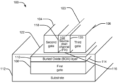
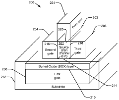
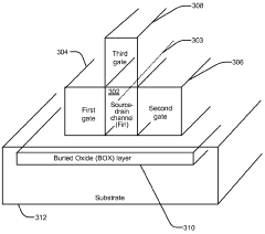
Fin-type device system and method
PatentWO2011028796A1
Innovation
- The use of FinFET transistors with three independently biasable gates, where the first gate is coupled to the fin through a buried oxide layer, allows for lower bias voltage operation during the HOLD phase, thereby increasing the time between memory refreshes and reducing power consumption.
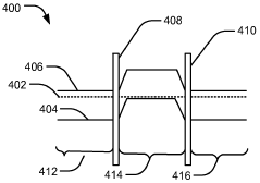
Multiple dielectric finfet structure and method
PatentInactiveUS20070290250A1
Innovation
- A method of forming FinFETs with multiple gate dielectric thicknesses by patterning fins, applying a first gate dielectric, protecting some fins with a mask, removing it from others, and adding additional dielectric layers to achieve varying thicknesses, allowing for optimized performance and reliability across different regions.
Thermal Management Strategies for Dense FinFET Layouts
As FinFET technology continues to scale down to meet the demands of modern integrated circuits, thermal management has become a critical challenge in dense layout designs. The compact arrangement of multiple FinFETs in limited space creates significant heat concentration that can compromise device performance, reliability, and lifespan. Effective thermal management strategies are therefore essential for optimizing FinFET layouts under space constraints.
Heat dissipation in densely packed FinFET structures requires multi-faceted approaches. Advanced materials with superior thermal conductivity properties are increasingly being incorporated into FinFET designs. Silicon-on-insulator (SOI) substrates with modified buried oxide layers help reduce thermal resistance, while high thermal conductivity materials like diamond or graphene-based compounds are being explored as heat spreaders in critical areas.
Layout-level thermal optimization techniques have proven particularly effective. Strategic placement of thermal vias and increased metal routing density in high-temperature regions facilitate heat transfer away from active devices. Implementation of thermal-aware cell placement algorithms that distribute heat-generating components more evenly across the die has shown to reduce hotspot formation by up to 30% in recent studies.
Dynamic thermal management systems represent another frontier in addressing thermal challenges. These systems incorporate on-chip temperature sensors strategically positioned near high-activity FinFET clusters to provide real-time thermal monitoring. When coupled with intelligent power management controllers, they can dynamically adjust operating frequencies or temporarily deactivate non-critical circuit blocks to prevent thermal runaway conditions.
3D integration techniques offer promising solutions for thermal management in space-constrained environments. Through-silicon vias (TSVs) not only provide electrical connections between stacked dies but also serve as efficient thermal conduits. Recent research demonstrates that properly designed TSV arrays can reduce peak temperatures by up to 15°C in multi-layer FinFET structures.
Liquid cooling technologies are gaining traction for extreme thermal management scenarios. Microfluidic channels integrated directly into the silicon substrate or interposer layers can remove heat more efficiently than traditional air cooling methods. Though implementation challenges remain, this approach has demonstrated cooling capabilities exceeding 500 W/cm² in laboratory settings, making it viable for ultra-dense FinFET deployments.
Computational fluid dynamics (CFD) modeling has become an indispensable tool in thermal management strategy development. Advanced simulation platforms now enable accurate prediction of thermal profiles in complex FinFET layouts before physical implementation, allowing designers to identify and mitigate potential hotspots early in the design process, reducing costly redesign cycles.
Manufacturing Considerations for Optimized FinFET Designs
Manufacturing FinFET devices with optimized layouts requires careful consideration of various fabrication constraints and process limitations. The semiconductor manufacturing process for FinFET structures involves complex lithography, etching, and deposition steps that directly impact device performance and yield. When optimizing FinFET layouts for space constraints, manufacturers must balance theoretical design goals with practical manufacturing capabilities.
Critical dimension (CD) control represents one of the primary manufacturing challenges in FinFET production. As fin widths continue to shrink below 10nm, maintaining consistent fin dimensions across the wafer becomes increasingly difficult. Process variations can lead to non-uniform threshold voltages and drive currents, degrading overall circuit performance. Advanced lithography techniques such as multiple patterning and EUV (Extreme Ultraviolet) lithography have been developed to address these challenges, though they add complexity and cost to the manufacturing process.
Fin pitch scaling presents another significant consideration. While reducing fin pitch allows for higher transistor density, it also increases the risk of fin collapse during wet processing steps. Manufacturers typically implement structural support features and modified etch recipes to maintain fin integrity at reduced pitches. Additionally, the aspect ratio of fins must be carefully controlled to balance performance benefits with structural stability during fabrication.
Metal gate formation and work function metal deposition represent critical steps that impact FinFET performance characteristics. The replacement metal gate process requires precise control of metal deposition thickness and uniformity. Variations in these parameters can lead to threshold voltage shifts and performance degradation. Manufacturers often implement tight process controls and in-line metrology to ensure consistency in these critical steps.
Source/drain epitaxial growth presents unique challenges in space-constrained layouts. The selective epitaxial growth process must accommodate reduced spacing between adjacent fins while maintaining proper dopant profiles. Manufacturers have developed specialized epitaxial recipes and growth conditions to achieve uniform material deposition in high-density fin arrangements.
Contact formation becomes increasingly challenging as device dimensions shrink. Self-aligned contact schemes have been widely adopted to address overlay issues, but they introduce additional process complexity. Advanced contact materials and deposition techniques are continuously being developed to reduce contact resistance while maintaining compatibility with scaled dimensions.
Defect density management remains a persistent challenge in FinFET manufacturing. Process-induced defects such as fin damage, gate oxide breakdown, and metal contamination can significantly impact yield. Manufacturers implement comprehensive defect reduction strategies, including clean room protocols, advanced filtration systems, and in-line inspection techniques to identify and mitigate defect sources throughout the fabrication process.
Unlock deeper insights with PatSnap Eureka Quick Research — get a full tech report to explore trends and direct your research. Try now!
Generate Your Research Report Instantly with AI Agent
Supercharge your innovation with PatSnap Eureka AI Agent Platform!