FinFET Vs Nanowire: Which Achieves Higher Scalability?
SEP 11, 202510 MIN READ
Generate Your Research Report Instantly with AI Agent
Patsnap Eureka helps you evaluate technical feasibility & market potential.
FinFET and Nanowire Evolution Background
The evolution of transistor technology has been driven by the semiconductor industry's relentless pursuit of Moore's Law, which predicts the doubling of transistor density approximately every two years. Since the 1960s, planar transistors dominated chip manufacturing until reaching physical limitations in the early 2000s. The introduction of FinFET technology around 2011 marked a revolutionary shift from planar to three-dimensional transistor architecture, enabling continued scaling beyond the 22nm node.
FinFET (Fin Field-Effect Transistor) technology emerged as a solution to the short-channel effects that plagued traditional planar transistors at smaller nodes. By raising the channel into a fin-like structure surrounded by the gate on three sides, FinFETs provided superior electrostatic control, reduced leakage current, and allowed for higher performance at lower operating voltages. Intel's introduction of "Tri-Gate" transistors (their implementation of FinFET) in 2011 at the 22nm node demonstrated the commercial viability of this approach.
The industry rapidly adopted FinFET technology, with major foundries like TSMC, Samsung, and GlobalFoundries implementing their versions at various nodes from 16/14nm down to 7nm. Each generation brought refinements in fin geometry, gate materials, and manufacturing processes, pushing the performance and efficiency boundaries further. However, as dimensions continued to shrink below 7nm, even FinFETs began encountering fundamental physical limitations.
This led to the development of nanowire (or nanosheet) transistor technology, representing the next evolutionary step. Nanowire transistors extend the multi-gate concept of FinFETs by completely surrounding the channel with the gate material, creating a gate-all-around (GAA) structure. This configuration offers even better electrostatic control than FinFETs, making it particularly suitable for nodes at 3nm and below.
Samsung announced its nanowire implementation called Multi-Bridge-Channel FET (MBCFET) in 2019, while TSMC and Intel have been developing their own versions. The transition from FinFET to nanowire represents not just an incremental improvement but a fundamental architectural shift necessary to maintain the scaling trajectory.
Both technologies share common ancestry in multi-gate transistor concepts first proposed in academic research during the 1990s. The progression from planar to FinFET to nanowire demonstrates the semiconductor industry's ability to overcome seemingly insurmountable physical barriers through architectural innovation rather than relying solely on dimensional scaling.
The evolution timeline shows accelerating development cycles, with research concepts moving to production more rapidly as competitive pressures intensify. This historical context is crucial for understanding the current scalability comparison between FinFET and nanowire technologies, as each represents a different point on the same evolutionary continuum of transistor architecture.
Market Demand Analysis for Advanced Transistor Technologies
The semiconductor industry's demand for advanced transistor technologies continues to be driven by the relentless pursuit of Moore's Law, which has historically guided chip development toward smaller, faster, and more energy-efficient designs. As traditional planar transistors reached their physical scaling limits around the 28nm node, FinFET technology emerged as the dominant architecture, enabling continued scaling down to the 5nm node. However, market analysis indicates that FinFET is now approaching its own scaling limitations, creating substantial demand for next-generation transistor technologies like nanowire (or gate-all-around) architectures.
Market research from leading semiconductor intelligence firms projects the global advanced transistor technology market to grow significantly through 2030, with particular acceleration in demand for sub-3nm process nodes where nanowire architectures demonstrate clear advantages. This growth is primarily fueled by expanding applications in high-performance computing, artificial intelligence, autonomous systems, and mobile devices requiring both increased computational power and improved energy efficiency.
Consumer electronics manufacturers are particularly vocal about their requirements for more efficient transistor technologies, as battery life remains a critical differentiator in mobile devices. Data centers and cloud service providers represent another major market segment driving demand for advanced transistor technologies, as they face mounting pressure to reduce energy consumption while handling exponentially growing computational workloads.
The automotive and industrial IoT sectors are emerging as significant new markets for advanced transistor technologies. These applications demand not only performance improvements but also enhanced reliability under harsh operating conditions, creating specialized market niches where the superior electrostatic control of nanowire architectures may provide compelling advantages over FinFET designs.
Regional market analysis reveals that East Asia continues to dominate demand for advanced transistor technologies, with Taiwan, South Korea, and increasingly China investing heavily in semiconductor manufacturing capabilities. North America maintains strong demand driven by cloud computing infrastructure and AI development, while Europe shows growing interest particularly for automotive and industrial applications.
Market forecasts indicate that the transition from FinFET to nanowire architectures will accelerate between 2023-2027, with early adoption in premium segments before broader implementation. This transition is expected to create significant opportunities for equipment manufacturers, materials suppliers, and design tool developers who can address the unique challenges of nanowire fabrication and integration.
Customer surveys across multiple industries consistently highlight three primary demands driving the market: power efficiency improvements of at least 30% over previous generations, continued performance scaling to support next-generation applications, and cost-effective manufacturing processes that can maintain reasonable yields at advanced nodes.
Current Scalability Challenges in Semiconductor Technology
The semiconductor industry has been driven by Moore's Law for decades, but as transistor dimensions approach atomic scale, fundamental physical limitations are creating unprecedented scalability challenges. Traditional planar transistors reached their scaling limits around the 28nm node, primarily due to short-channel effects (SCEs) that cause increased leakage current and poor electrostatic control. These limitations prompted the industry's shift to three-dimensional architectures, with FinFET technology emerging as the dominant solution since the 22nm node.
Despite FinFET's success in extending Moore's Law, the technology is now encountering its own scaling barriers as dimensions continue to shrink below 5nm. Quantum tunneling effects become increasingly problematic at these dimensions, while variability in manufacturing processes leads to inconsistent device performance. Additionally, the fin width cannot be scaled indefinitely without compromising structural integrity and current-carrying capability.
Power density has emerged as another critical challenge, with smaller transistors generating more heat per unit area. This thermal constraint is particularly problematic in high-performance computing applications where power efficiency directly impacts system performance. The industry is approaching fundamental thermodynamic limits that cannot be overcome through traditional scaling approaches alone.
Contact resistance represents a growing proportion of total device resistance as dimensions shrink, creating a bottleneck for performance improvements. The interface between the semiconductor and metal contacts becomes increasingly critical, with atomic-level precision required for optimal performance. This challenge is compounded by the limited options for compatible materials that can maintain low resistance at nanoscale dimensions.
Gate oxide scaling has essentially reached its physical limit with conventional materials, as electron tunneling becomes dominant below approximately 0.7nm thickness. While high-k dielectric materials provided temporary relief, the industry requires new material systems and gate stack architectures to enable further scaling without compromising reliability or performance.
Lithography challenges persist despite advances in extreme ultraviolet (EUV) technology. Multi-patterning techniques add complexity and cost to manufacturing processes, while edge placement errors become increasingly problematic at smaller dimensions. The precision required for advanced nodes pushes the boundaries of metrology capabilities, making process control exceptionally difficult.
These combined challenges have created an inflection point in semiconductor technology, driving the exploration of alternative architectures like Gate-All-Around (GAA) nanowire transistors. The fundamental question of whether FinFET technology can be further optimized or if nanowire structures represent the necessary evolutionary step has become central to the industry's roadmap for continued scaling beyond the 3nm node.
Technical Comparison of FinFET vs Nanowire Solutions
01 FinFET scaling advantages and limitations
FinFET technology offers improved scalability compared to traditional planar transistors due to better electrostatic control of the channel. The three-dimensional fin structure reduces short-channel effects and allows for continued scaling to smaller nodes. However, FinFETs face limitations at extreme scaling nodes due to fin width control challenges and increased parasitic capacitance. These limitations affect performance and power efficiency as dimensions shrink below certain thresholds.- FinFET scaling advantages and limitations: FinFET technology offers improved scalability compared to planar transistors due to better electrostatic control of the channel. The multi-gate structure reduces short channel effects and leakage current, allowing for continued scaling to smaller nodes. However, FinFETs face limitations at extreme scaling, including fin width variability, increased parasitic capacitance, and challenges in maintaining effective channel control as dimensions shrink below certain thresholds.
- Nanowire transistor architecture for advanced scaling: Nanowire transistors represent the next evolution beyond FinFETs for continued scaling. The gate-all-around structure provides superior electrostatic control of the channel from all sides, enabling further miniaturization. Nanowire designs can achieve better performance at smaller dimensions with reduced short channel effects and improved carrier mobility. These structures allow for more efficient use of space on the chip while maintaining or improving electrical characteristics.
- Fabrication techniques for scalable transistor structures: Advanced fabrication methods are critical for scaling both FinFET and nanowire transistors. These include selective epitaxial growth for channel materials, atomic layer deposition for ultra-thin gate dielectrics, and advanced lithography techniques. Self-aligned processes help minimize variability in critical dimensions, while strain engineering enhances carrier mobility. Novel etching and deposition methods enable the creation of increasingly complex 3D structures with the precision required for nanoscale devices.
- Materials innovation for transistor scaling: Novel materials are essential for overcoming scaling limitations in advanced transistor architectures. High-k dielectrics reduce gate leakage while maintaining equivalent oxide thickness. Channel materials with higher carrier mobility, such as silicon-germanium, germanium, and III-V compounds, enable better performance at smaller dimensions. Metal gate materials with appropriate work functions optimize threshold voltages. These material innovations address fundamental physical limitations that emerge as device dimensions approach atomic scales.
- Modeling and simulation approaches for nanoscale transistors: Computational modeling and simulation tools are crucial for understanding and optimizing the scalability of advanced transistor architectures. Quantum mechanical effects become increasingly important at nanoscale dimensions and must be accurately modeled. Multi-scale simulation approaches combine atomistic, quantum, and device-level models to predict performance and identify scaling bottlenecks. These tools enable virtual prototyping of novel device structures and materials before expensive fabrication, accelerating the development of more scalable transistor technologies.
02 Nanowire transistor architecture for advanced scaling
Nanowire transistors represent the next evolution beyond FinFETs for continued scaling. The gate-all-around architecture provides superior electrostatic control by surrounding the channel completely, enabling effective scaling to smaller dimensions. Nanowire designs can incorporate multiple stacked channels to increase current drive while maintaining a small footprint. This architecture significantly reduces short-channel effects and allows for continued scaling beyond what is possible with FinFET technology.Expand Specific Solutions03 Fabrication techniques for scalable transistor structures
Advanced fabrication methods are crucial for scaling both FinFET and nanowire transistors. These include selective epitaxial growth for channel formation, atomic layer deposition for uniform gate dielectric coverage, and self-aligned processes to minimize variability. Novel etching techniques enable the creation of high-aspect-ratio fins and suspended nanowire channels. These fabrication approaches address critical dimensional control challenges that arise when scaling to smaller nodes.Expand Specific Solutions04 Materials innovation for transistor scaling
Novel materials are essential for overcoming scaling limitations in advanced transistor architectures. High-mobility channel materials like silicon-germanium, germanium, and III-V compounds enhance carrier transport in scaled devices. High-k dielectric materials and metal gates improve electrostatic control while reducing leakage current. Strain engineering techniques modify the electronic band structure to enhance carrier mobility in highly scaled channels, improving performance at smaller dimensions.Expand Specific Solutions05 Modeling and simulation approaches for scaled transistors
Computational modeling and simulation tools are critical for predicting the performance of highly scaled transistor structures. Advanced TCAD (Technology Computer-Aided Design) simulations incorporate quantum effects that become significant at nanoscale dimensions. Multi-physics modeling approaches account for electrostatic, thermal, and mechanical interactions in complex 3D architectures. These simulation techniques guide design optimization and help identify scaling limitations before fabrication, accelerating the development of next-generation transistor technologies.Expand Specific Solutions
Key Semiconductor Players and Competitive Landscape
The FinFET vs Nanowire scalability competition represents a critical transition in semiconductor technology, currently in the mature-to-advanced development phase. The global semiconductor foundry market, valued at approximately $100 billion, is witnessing major players positioning themselves strategically in this technological evolution. Leading companies like TSMC, Samsung, and Intel are heavily investing in nanowire/nanosheet technology as FinFET approaches its scaling limits around 5nm. IBM has demonstrated significant breakthroughs in nanowire architecture, while GLOBALFOUNDRIES and SMIC are working to close the technology gap. Academic institutions including Peking University and Chinese Academy of Sciences are contributing fundamental research to advance nanowire technology, which offers superior electrostatic control and reduced short-channel effects compared to FinFET, making it the likely successor for sub-5nm nodes.
International Business Machines Corp.
Technical Solution: IBM has pioneered nanowire technology with their Gate-All-Around (GAA) architecture, specifically through their Nanosheet FET design. IBM's approach utilizes multiple stacked silicon nanosheets with gate material surrounding each sheet, providing enhanced electrostatic control compared to FinFET. Their 5nm GAA technology demonstrates a 40% performance improvement at fixed power or 75% power reduction at matched performance versus 10nm FinFET[1]. IBM's nanowire implementation allows for variable nanosheet widths within the same manufacturing process, enabling fine-tuning of power and performance characteristics. Their research shows nanowire transistors can scale to 3nm and potentially beyond, while FinFETs face significant challenges below 5nm due to short-channel effects and increasing leakage currents[2]. IBM has collaborated with Samsung and GlobalFoundries through their Research Alliance to accelerate this technology's development.
Strengths: Superior electrostatic control enabling continued scaling beyond FinFET limitations; flexibility in performance tuning through variable nanosheet widths; demonstrated path to 3nm and below. Weaknesses: More complex manufacturing process requiring precise material deposition and etching; higher initial production costs; challenges in managing parasitic capacitance between stacked nanosheets.
Taiwan Semiconductor Manufacturing Co., Ltd.
Technical Solution: TSMC has developed a comprehensive approach to transistor scaling, evaluating both advanced FinFET and nanosheet/nanowire technologies. For FinFET, TSMC has pushed the architecture to its limits with their N5 and N3 process nodes, implementing super high-density designs with reduced fin pitch and height optimization. Their FinFET technology at 3nm achieves approximately 70% logic density improvement and 15% speed gain compared to 5nm[3]. However, recognizing FinFET's scaling limitations, TSMC is transitioning to their Gate-All-Around (GAA) nanosheet technology for future nodes. Their GAA implementation features horizontally stacked silicon nanosheets with surrounding gate material, providing 360-degree electrostatic control. TSMC's research indicates their nanosheet design can achieve 30% better drive current than FinFET at the same leakage levels[4]. The company has also explored innovative channel materials like germanium and III-V semiconductors to further enhance nanowire performance for sub-3nm nodes.
Strengths: Industry-leading manufacturing expertise allowing optimization of both architectures; demonstrated high-volume production capability for advanced nodes; comprehensive materials research enabling performance enhancements. Weaknesses: FinFET approach facing fundamental scaling limits below 3nm; transition to nanowire requires significant manufacturing process changes; higher initial production costs for nanowire implementation.
Critical Patents and Research in Transistor Scaling
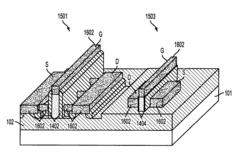
Nanowire FET and finfet
PatentInactiveUS20130341596A1
Innovation
- A CMOS device is fabricated with a buried oxide layer, featuring nanowire FETs with suspended nanowires and pads, and finFETs with multiple fins, both with gate stacks that define channel regions, allowing for improved scaling and performance through specific fabrication processes including etching, epitaxial growth, and silicide formation.
Power Efficiency and Performance Trade-offs
Power efficiency and performance represent critical considerations in the comparison between FinFET and nanowire transistor technologies. FinFETs have dominated semiconductor manufacturing for several generations, offering significant improvements over planar transistors in terms of power consumption and performance. However, as scaling continues toward sub-5nm nodes, the fundamental limitations of FinFET architecture become increasingly apparent.
FinFET technology demonstrates excellent power efficiency at larger nodes (14nm-7nm) due to its three-dimensional gate structure that provides superior electrostatic control over the channel. This results in reduced leakage current and lower static power consumption compared to planar transistors. The multi-gate design allows for operation at lower threshold voltages while maintaining acceptable leakage characteristics, enabling dynamic power reduction through voltage scaling.
Nanowire transistors (particularly Gate-All-Around or GAA designs) take this electrostatic control further by completely surrounding the channel with the gate material. This configuration provides nearly ideal subthreshold characteristics with minimal short-channel effects even at extremely scaled dimensions. Consequently, nanowire architectures can operate at lower supply voltages than equivalent FinFETs, potentially reducing dynamic power consumption by 10-25% according to recent industry reports.
Performance metrics reveal interesting trade-offs between these technologies. FinFETs generally exhibit higher carrier mobility in current implementations, particularly for NMOS transistors, resulting in better raw performance at equivalent process nodes. This advantage stems from years of manufacturing optimization and strain engineering techniques specifically developed for fin structures.
Nanowire transistors initially may show lower drive currents per device width compared to FinFETs. However, their superior scalability allows for more efficient use of silicon area, potentially enabling higher transistor densities and therefore greater overall chip performance. Additionally, nanowire structures permit more flexible channel material engineering, including the incorporation of high-mobility materials like germanium or III-V compounds.
The performance-power envelope evolves differently for each technology across scaling nodes. FinFETs face increasing challenges maintaining their power efficiency advantages below 5nm, as fin widths become difficult to control precisely. Nanowires demonstrate more favorable scaling characteristics, maintaining their power efficiency advantages even at extreme dimensions, though with higher manufacturing complexity.
Industry benchmarks suggest that at 3nm and below, nanowire-based GAA transistors offer approximately 30% better power efficiency at equivalent performance levels compared to scaled FinFETs. This advantage becomes particularly significant for mobile and IoT applications where battery life is paramount, potentially extending operational time by 15-20% in typical usage scenarios.
Manufacturing Complexity and Cost Analysis
Manufacturing complexity and cost analysis represent critical factors in determining the commercial viability of semiconductor technologies. FinFET technology, while established in production environments, presents significant manufacturing challenges as scaling continues below 7nm. The multi-gate 3D structure requires precise fin formation with extremely tight dimensional control, increasing lithography complexity and manufacturing costs with each node advancement.
The fabrication of FinFETs demands sophisticated multi-patterning techniques at advanced nodes, with some manufacturers implementing expensive extreme ultraviolet (EUV) lithography to maintain yield rates. The vertical fin structure necessitates complex etching processes with high aspect ratios, leading to increased production cycle times and equipment requirements. Additionally, the doping of these tall, narrow fins presents uniformity challenges that impact device performance consistency.
Nanowire (or Gate-All-Around) technology introduces even greater manufacturing complexity initially, requiring precise formation of suspended silicon channels completely surrounded by gate material. The fabrication process involves additional steps for channel release and gate material deposition around the entire wire structure. This increased process complexity translates to higher initial manufacturing costs and potentially lower yields during early production phases.
However, nanowire technology offers potential cost advantages at extreme scaling nodes (3nm and below). The inherent design allows for more straightforward dimensional scaling without the structural limitations of fins. Industry analysis suggests that while initial implementation costs are higher, the longer-term scaling path may present better economics as FinFET manufacturing becomes prohibitively complex at dimensions below 3nm.
Equipment requirements differ significantly between the technologies. FinFET production at advanced nodes requires substantial capital investment in precision lithography and etching tools. Nanowire fabrication demands these same tools plus specialized equipment for channel formation and gate deposition processes. TSMC and Samsung have reported capital expenditure increases of 15-25% for initial nanowire implementation compared to equivalent FinFET nodes.
Yield management represents another critical cost factor. FinFET technology benefits from manufacturing maturity with established defect control mechanisms. Nanowire technology currently experiences lower initial yields, though this gap is expected to narrow as manufacturing processes mature. Economic modeling from semiconductor equipment suppliers indicates that the crossover point where nanowire becomes more cost-effective than FinFET likely occurs around the 3nm to 2nm transition, aligning with the physical scaling limitations of FinFET architecture.
Unlock deeper insights with Patsnap Eureka Quick Research — get a full tech report to explore trends and direct your research. Try now!
Generate Your Research Report Instantly with AI Agent
Supercharge your innovation with Patsnap Eureka AI Agent Platform!