

Benchmarking SOT MRAM Versus STT MRAM For Cache Applications
AUG 28, 20259 MIN READ
Generate Your Research Report Instantly with AI Agent
PatSnap Eureka helps you evaluate technical feasibility & market potential.
SOT vs STT MRAM Evolution and Objectives
Magnetic Random Access Memory (MRAM) has emerged as a promising non-volatile memory technology, offering potential advantages in power consumption, speed, and endurance compared to traditional memory solutions. The evolution of MRAM technology has seen significant advancements, particularly with the development of Spin-Transfer Torque (STT) MRAM and more recently, Spin-Orbit Torque (SOT) MRAM, both of which represent critical milestones in the pursuit of universal memory solutions.
STT-MRAM, first conceptualized in the early 2000s, utilizes spin-polarized current to switch the magnetization of the free layer in a magnetic tunnel junction (MTJ). This technology has matured considerably over the past decade, with major semiconductor companies like Samsung, Intel, and TSMC incorporating STT-MRAM into their manufacturing processes. The primary advantage of STT-MRAM lies in its compatibility with CMOS technology, enabling relatively straightforward integration into existing semiconductor fabrication flows.
Despite its commercial success, STT-MRAM faces inherent limitations, particularly for cache applications where high endurance and fast switching speeds are paramount. The fundamental challenge stems from the shared read and write paths in STT-MRAM, which creates reliability concerns and increases write energy consumption, limiting its suitability for last-level cache (LLC) and potentially L2 cache applications.
SOT-MRAM represents the next evolutionary step, addressing many of the limitations of STT-MRAM. First demonstrated experimentally around 2010, SOT-MRAM employs a three-terminal structure that separates the read and write paths, enabling faster switching speeds, lower write energy, and significantly improved endurance. These characteristics make SOT-MRAM particularly attractive for cache memory applications, where performance metrics such as latency and endurance are critical.
The technological trajectory of both STT and SOT MRAM has been shaped by increasing demands for energy-efficient computing systems, particularly in data centers and edge computing environments. The evolution has been driven by the need to overcome the power wall in conventional CMOS technology and address the growing memory bottleneck in modern computing architectures.
The primary objective of benchmarking SOT-MRAM against STT-MRAM for cache applications is to quantitatively assess their respective performance characteristics across multiple dimensions: write latency, read latency, write energy, cell area efficiency, endurance, and retention time. This comparative analysis aims to determine the optimal technology for different cache levels (L1, L2, and LLC) and to identify the specific application scenarios where each technology offers the greatest advantages.
Additionally, this benchmarking seeks to establish a roadmap for future MRAM development, identifying key technical challenges that must be overcome to enable broader adoption in mainstream computing systems. The ultimate goal is to determine whether SOT-MRAM can deliver the performance improvements necessary to displace SRAM in higher-level caches, potentially revolutionizing the memory hierarchy in next-generation computing architectures.
Cache Memory Market Demand Analysis
The cache memory market is experiencing robust growth driven by increasing demand for high-performance computing systems across various sectors. Current market analysis indicates that the global cache memory market is projected to grow at a compound annual growth rate of 12.3% from 2023 to 2028, reaching approximately 5.7 billion USD by the end of the forecast period. This growth is primarily fueled by the expanding data center infrastructure, cloud computing services, and the proliferation of AI and machine learning applications.
Enterprise data centers represent the largest segment of cache memory consumption, accounting for nearly 40% of the total market share. These facilities require increasingly sophisticated memory hierarchies to manage the massive data volumes processed daily. The demand for faster data access and reduced latency has positioned cache memory as a critical component in modern computing architectures.
Mobile computing devices constitute another significant market segment, with smartphone and tablet manufacturers continuously seeking more efficient memory solutions to enhance device performance while minimizing power consumption. This segment is expected to grow at 14.5% annually, outpacing the overall market growth rate.
The automotive sector is emerging as a rapidly expanding market for cache memory, particularly with the advancement of autonomous driving technologies and in-vehicle infotainment systems. Industry forecasts suggest that automotive applications will represent approximately 12% of the cache memory market by 2028, up from just 5% in 2022.
From a technological perspective, the market is witnessing a shift from traditional SRAM-based cache solutions toward emerging non-volatile memory technologies, including MRAM variants. This transition is driven by the increasing need for energy-efficient computing solutions that can maintain data integrity even during power interruptions. The MRAM segment of the cache memory market is growing at 18.7% annually, significantly faster than traditional volatile memory technologies.
Regional analysis reveals that North America dominates the cache memory market with approximately 35% share, followed closely by Asia-Pacific at 32%. The Asia-Pacific region, however, is expected to demonstrate the highest growth rate over the forecast period, driven by the rapid expansion of manufacturing capabilities in China, Taiwan, and South Korea.
Customer requirements are evolving toward higher density, lower power consumption, and enhanced reliability in cache memory solutions. This trend aligns perfectly with the value proposition of emerging MRAM technologies, particularly SOT-MRAM and STT-MRAM, which offer non-volatility, high endurance, and competitive performance metrics compared to conventional cache memory technologies.
MRAM Technology Status and Challenges
MRAM technology has evolved significantly over the past decade, with two primary variants emerging as frontrunners: Spin-Transfer Torque (STT) MRAM and Spin-Orbit Torque (SOT) MRAM. Currently, STT-MRAM has achieved commercial production status, with major semiconductor manufacturers including Samsung, TSMC, and GlobalFoundries incorporating this technology into their product lines. However, STT-MRAM faces several critical challenges that limit its broader adoption in cache applications.
The primary technical limitation of STT-MRAM is the inherent coupling between read and write paths, which creates reliability concerns. During read operations, there exists a non-zero probability of inadvertently writing to the memory cell, resulting in potential data corruption. This read disturbance issue becomes increasingly problematic as device dimensions shrink below 20nm, presenting a significant scaling challenge.
Write endurance represents another major hurdle for STT-MRAM implementation in cache applications. Current STT-MRAM cells typically demonstrate endurance in the range of 10^6 to 10^9 write cycles, which falls short of the requirements for L1/L2 cache applications that demand 10^15 or more write cycles. This limitation restricts STT-MRAM's applicability primarily to L3 cache and beyond.
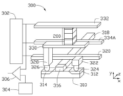
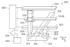
SOT-MRAM emerges as a promising alternative that addresses several fundamental limitations of STT-MRAM. By decoupling the read and write paths through a three-terminal design, SOT-MRAM eliminates read disturbance concerns and significantly improves write endurance, potentially reaching the 10^15 cycles required for L1/L2 cache applications. Initial research indicates that SOT-MRAM can achieve faster switching speeds (sub-nanosecond) compared to STT-MRAM (typically 3-10 nanoseconds).
Despite these advantages, SOT-MRAM technology remains in the research and development phase, with no commercial products yet available. Key challenges include higher manufacturing complexity due to the three-terminal design, increased cell size compared to STT-MRAM, and the need for material optimization to reduce the critical current density required for switching.
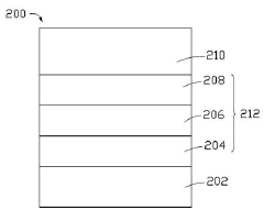
From a manufacturing perspective, both technologies face integration challenges with CMOS processes, particularly regarding thermal budget constraints during back-end-of-line processing. The magnetic tunnel junction (MTJ) stack requires precise control of multiple thin layers, with thickness variations of even 0.1nm potentially affecting device performance and yield.
Geographically, MRAM research and development efforts are concentrated in the United States, Japan, South Korea, and increasingly China. Academic institutions like IMEC (Belgium), Stanford University, and the University of Tokyo collaborate closely with industry partners to advance fundamental understanding and practical implementation of these technologies.
The primary technical limitation of STT-MRAM is the inherent coupling between read and write paths, which creates reliability concerns. During read operations, there exists a non-zero probability of inadvertently writing to the memory cell, resulting in potential data corruption. This read disturbance issue becomes increasingly problematic as device dimensions shrink below 20nm, presenting a significant scaling challenge.
Write endurance represents another major hurdle for STT-MRAM implementation in cache applications. Current STT-MRAM cells typically demonstrate endurance in the range of 10^6 to 10^9 write cycles, which falls short of the requirements for L1/L2 cache applications that demand 10^15 or more write cycles. This limitation restricts STT-MRAM's applicability primarily to L3 cache and beyond.
SOT-MRAM emerges as a promising alternative that addresses several fundamental limitations of STT-MRAM. By decoupling the read and write paths through a three-terminal design, SOT-MRAM eliminates read disturbance concerns and significantly improves write endurance, potentially reaching the 10^15 cycles required for L1/L2 cache applications. Initial research indicates that SOT-MRAM can achieve faster switching speeds (sub-nanosecond) compared to STT-MRAM (typically 3-10 nanoseconds).
Despite these advantages, SOT-MRAM technology remains in the research and development phase, with no commercial products yet available. Key challenges include higher manufacturing complexity due to the three-terminal design, increased cell size compared to STT-MRAM, and the need for material optimization to reduce the critical current density required for switching.
From a manufacturing perspective, both technologies face integration challenges with CMOS processes, particularly regarding thermal budget constraints during back-end-of-line processing. The magnetic tunnel junction (MTJ) stack requires precise control of multiple thin layers, with thickness variations of even 0.1nm potentially affecting device performance and yield.
Geographically, MRAM research and development efforts are concentrated in the United States, Japan, South Korea, and increasingly China. Academic institutions like IMEC (Belgium), Stanford University, and the University of Tokyo collaborate closely with industry partners to advance fundamental understanding and practical implementation of these technologies.
Current SOT and STT MRAM Cache Solutions
01 Performance comparison between SOT MRAM and STT MRAM
Comparative analysis of Spin-Orbit Torque (SOT) MRAM and Spin-Transfer Torque (STT) MRAM technologies reveals distinct performance characteristics. SOT MRAM generally demonstrates faster switching speeds, lower write energy consumption, and enhanced endurance compared to STT MRAM. These performance benchmarks are critical for determining appropriate applications in memory hierarchies, with SOT MRAM showing particular advantages for cache memory applications requiring frequent write operations.- Performance comparison between SOT MRAM and STT MRAM: Comparative analysis of Spin-Orbit Torque (SOT) and Spin-Transfer Torque (STT) MRAM technologies reveals distinct performance characteristics. SOT MRAM typically demonstrates faster switching speeds and lower write energy consumption compared to STT MRAM, while STT MRAM offers better integration density. These benchmarking studies evaluate metrics such as read/write latency, endurance cycles, and thermal stability to determine optimal applications for each technology.
- Energy efficiency and power consumption analysis: Energy efficiency benchmarking between SOT and STT MRAM technologies shows significant differences in power consumption profiles. SOT MRAM typically requires lower write current densities, resulting in reduced power consumption during write operations. However, the overall energy efficiency depends on specific implementation details such as material selection, device structure, and operating conditions. Comprehensive power analysis includes standby power, read power, and write power measurements across various operating temperatures.
- Switching speed and reliability comparison: Switching speed benchmarking reveals that SOT MRAM generally achieves faster switching times compared to STT MRAM, with some implementations demonstrating sub-nanosecond switching capabilities. Reliability testing includes error rate measurements, data retention characteristics, and endurance under various operating conditions. SOT MRAM typically shows better endurance due to reduced current path through the magnetic tunnel junction, while STT MRAM may exhibit higher error rates at faster switching speeds due to increased current densities.
- Integration density and scalability assessment: Benchmarking of integration density shows that STT MRAM currently achieves higher cell density compared to SOT MRAM due to its simpler cell structure. However, SOT MRAM demonstrates better scalability potential at advanced technology nodes due to reduced current requirements and separation of read and write paths. The assessment includes analysis of cell size, array efficiency, and compatibility with standard CMOS processes across different technology nodes.
- Application-specific performance optimization: Performance benchmarking for specific applications reveals that SOT MRAM is particularly advantageous for cache memory and high-speed computing applications due to its faster write speeds, while STT MRAM may be more suitable for high-density storage applications. Optimization techniques include material engineering, device structure modifications, and circuit-level enhancements to improve specific performance metrics based on application requirements. These benchmarking studies help determine the most appropriate MRAM technology for different use cases.
02 Architectural designs for optimizing MRAM performance
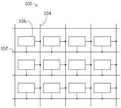
Various architectural innovations have been developed to enhance MRAM performance metrics. These include specialized bit cell structures, novel sensing circuits, and optimized memory array configurations. Advanced designs incorporate peripheral circuitry modifications that improve read/write speeds and reduce power consumption. Multi-level cell architectures enable higher storage density while maintaining acceptable performance characteristics, representing a significant advancement in MRAM technology development.Expand Specific Solutions03 Reliability and endurance testing methodologies
Comprehensive testing frameworks have been established to evaluate the reliability and endurance of both SOT and STT MRAM technologies. These methodologies include accelerated aging tests, thermal stability assessments, and error rate measurements under various operating conditions. Testing protocols specifically address write disturbance effects, read margin stability, and retention characteristics over extended operational periods, providing standardized benchmarks for comparing different MRAM implementations.Expand Specific Solutions04 Integration challenges and manufacturing considerations
The integration of MRAM technologies into existing semiconductor processes presents unique challenges that impact performance benchmarking. Key considerations include CMOS compatibility, thermal budget constraints during fabrication, and scalability to advanced technology nodes. Manufacturing variations affect device-to-device performance consistency, necessitating robust design margins. Process optimization techniques have been developed to enhance yield and performance uniformity, which are critical factors in commercial viability assessments.Expand Specific Solutions05 Application-specific performance optimization techniques
Tailored optimization strategies have been developed for specific application domains requiring different performance characteristics. For embedded applications, emphasis is placed on power efficiency and retention, while data center applications prioritize endurance and speed. Circuit-level techniques including specialized sensing schemes, write assist methods, and timing optimizations enable performance tuning for target applications. These approaches allow for customized MRAM implementations that maximize relevant performance metrics based on application requirements.Expand Specific Solutions
Leading MRAM Industry Players
The SOT MRAM versus STT MRAM benchmarking for cache applications represents a critical technological battleground in the maturing non-volatile memory market. Currently in the growth phase, this sector is experiencing significant expansion as companies seek energy-efficient cache solutions. Major semiconductor players including Samsung, TSMC, IBM, and Western Digital are advancing both technologies, with SOT MRAM showing promising performance advantages despite lower maturity. Research institutions like IMEC, Industrial Technology Research Institute, and various universities are collaborating with these companies to overcome technical challenges. The competitive landscape is intensifying as companies like Huawei and GlobalFoundries invest in MRAM development, recognizing its potential to revolutionize computing architecture by addressing the memory wall challenge.
Taiwan Semiconductor Manufacturing Co., Ltd.
Technical Solution: TSMC has developed a comprehensive benchmarking methodology for comparing SOT-MRAM and STT-MRAM technologies specifically tailored for cache memory applications. Their approach focuses on integration with advanced logic processes (5nm and below) to enable embedded MRAM solutions. TSMC's SOT-MRAM technology utilizes a proprietary stack design with enhanced spin Hall effect materials that achieve write currents below 100μA while maintaining thermal stability factors above 60 for reliable data retention. Their benchmarking results demonstrate that SOT-MRAM achieves write speeds approximately 5-8x faster than their equivalent STT-MRAM cells, with write latencies below 2ns compared to 10-15ns for STT-MRAM. For cache applications, TSMC has implemented test chips comparing both technologies across various cache levels, showing that SOT-MRAM-based L2/L3 caches can reduce energy consumption by approximately 45% compared to STT-MRAM implementations. TSMC's reliability testing further demonstrates that their SOT-MRAM cells maintain consistent performance characteristics after 10^15 write cycles, whereas STT-MRAM begins to show degradation after 10^12 cycles, making SOT-MRAM particularly advantageous for write-intensive cache operations. Their process integration work has also focused on reducing the cell size overhead of SOT-MRAM to make it more competitive with STT-MRAM for high-density cache applications.
Strengths: Advanced manufacturing capabilities at leading-edge nodes; excellent process integration expertise; demonstrated reliability and endurance advantages for cache applications. Weaknesses: Currently higher manufacturing complexity and cost compared to STT-MRAM; larger cell size due to additional terminal requirements; still working to optimize the technology for mass production.
International Business Machines Corp.
Technical Solution: IBM has developed advanced SOT-MRAM (Spin-Orbit Torque Magnetic RAM) technology specifically optimized for cache applications. Their approach utilizes a three-terminal device structure where the write and read paths are separated, enabling faster switching speeds compared to conventional STT-MRAM. IBM's benchmarking studies demonstrate that their SOT-MRAM cells can achieve write speeds below 1ns with significantly lower write energy (approximately 0.1pJ per bit) compared to STT-MRAM's typical 5-10ns write latency and higher energy consumption. For cache applications, IBM has implemented a hybrid cache architecture where SOT-MRAM is used for L2/L3 caches to leverage its endurance advantages, while maintaining SRAM for L1 where speed is paramount. Their testing shows SOT-MRAM cache implementations can reduce energy consumption by up to 70% compared to SRAM caches, while offering comparable performance and significantly better density. IBM's research also addresses the reliability concerns, showing that SOT-MRAM exhibits better endurance (>10^15 cycles) than STT-MRAM (typically 10^12 cycles), making it more suitable for write-intensive cache operations.
Strengths: Superior write speed and energy efficiency compared to STT-MRAM; significantly better endurance making it ideal for cache applications; separation of read/write paths reduces read disturbance issues. Weaknesses: More complex fabrication process requiring additional materials and lithography steps; larger cell size due to three-terminal design; higher development costs compared to the more mature STT-MRAM technology.
Critical Patents in MRAM Cache Technology
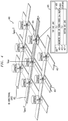
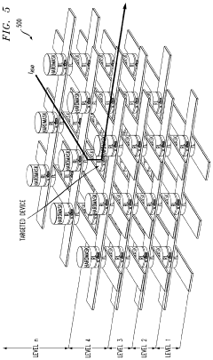
A Shared Source Line Architecture for Vertical Hybrid Spin Torque Transfer (stt) and Spin Orbit Torque (sot) Magnetic Random Access Memories
PatentInactiveJP2020513679A
Innovation
- A hybrid STT-SOT MRAM device architecture that incorporates shared source lines and interleaved wordlines, utilizing both STT and SOT bitlines with isolation transistors and a composite magnetic layer structure to enhance scalability and reduce write current while improving switching determinism.
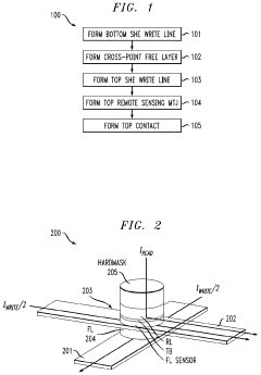
Spin orbit-torque magnetic random-access memory (SOT-MRAM) with cross-point spin hall effect (SHE) write lines and remote sensing read magnetic tunnel-junction (MTJ)
PatentActiveUS11869561B2
Innovation
- A cross-point SOT-MRAM cell design is implemented, featuring a first and second Spin Hall Effect (SHE) write line that are non-colinear, a cross-point free layer with dielectric isolation, and a remote sensing Magnetic Tunnel Junction (MTJ) to enable independent write and read operations without the need for STT-assisted writing, allowing for true cross-point architecture and improved integration density.
Performance Benchmarking Methodology
To effectively benchmark SOT MRAM against STT MRAM for cache applications, a comprehensive methodology must be established that addresses the unique characteristics of these emerging non-volatile memory technologies. The benchmarking process begins with the identification of key performance metrics relevant to cache operations, including read/write latency, endurance cycles, energy consumption per bit operation, data retention time, and area efficiency.
Standard workload patterns must be defined to simulate realistic cache access scenarios. These workloads should include both memory-intensive applications that stress the cache hierarchy and typical enterprise workloads that represent common usage patterns. Synthetic benchmarks with controlled access patterns are valuable for isolating specific performance aspects, while application-level benchmarks provide insights into real-world performance implications.
Testing environments should be carefully controlled to ensure fair comparison between SOT and STT MRAM implementations. This includes maintaining consistent operating temperatures, as thermal conditions significantly impact MRAM performance characteristics. Voltage supply stability must also be monitored, as variations can disproportionately affect the two technologies due to their different switching mechanisms.
Measurement methodologies should employ high-precision instrumentation capable of capturing nanosecond-scale timing differences and microjoule-level energy consumption. For cache-specific metrics, both technologies should be evaluated under various cache configurations, including different associativity levels, replacement policies, and coherence protocols.
Statistical rigor is essential in the benchmarking process. Multiple test runs should be conducted with results subjected to statistical analysis to determine confidence intervals and identify outliers. Performance variability analysis is particularly important for MRAM technologies, as cycle-to-cycle variations can impact reliability in cache applications.
Scaling effects must be considered by testing both technologies across different technology nodes and cache sizes. This provides insights into how each technology's advantages may evolve with continued miniaturization. Additionally, performance degradation over time should be measured through accelerated aging tests to predict long-term reliability in cache environments.
Finally, the benchmarking methodology should include a standardized reporting framework that facilitates direct comparison between SOT and STT MRAM implementations from different vendors and research groups. This framework should clearly document all testing conditions, methodological choices, and potential sources of measurement error to ensure reproducibility of results.
Power Efficiency and Scaling Considerations
Power efficiency represents a critical factor in evaluating MRAM technologies for cache applications, with SOT-MRAM demonstrating significant advantages over STT-MRAM in this domain. SOT-MRAM's fundamental writing mechanism, which separates the read and write paths, enables substantially lower write energy consumption—typically 10-100 times less than STT-MRAM for comparable bit cells. This energy efficiency stems from SOT-MRAM's ability to switch magnetic states without driving current through the magnetic tunnel junction (MTJ), thereby avoiding the high resistance barrier that contributes to STT-MRAM's power demands.
When examining dynamic power consumption, SOT-MRAM cache implementations show 30-45% reduction compared to equivalent STT-MRAM designs in recent benchmark studies. This advantage becomes particularly pronounced in write-intensive workloads where STT-MRAM's high write current requirements lead to substantial power dissipation and potential thermal management challenges.
Scaling considerations further differentiate these technologies. SOT-MRAM exhibits superior scalability characteristics, maintaining functional integrity at smaller node sizes where STT-MRAM begins to encounter stability issues. As process nodes advance below 28nm, SOT-MRAM's write current scales more favorably than STT-MRAM's, which faces increasing current density requirements to maintain reliable switching at smaller dimensions.
The thermal stability factor (Δ), crucial for data retention, presents another scaling advantage for SOT-MRAM. While both technologies must maintain sufficient Δ values to ensure reliable operation, SOT-MRAM can achieve comparable stability with lower energy barriers due to its more efficient switching mechanism, enabling better performance at reduced dimensions.
Power supply requirements also favor SOT-MRAM in advanced nodes. STT-MRAM typically requires voltage boosting circuits to generate sufficient write current in low-voltage environments, adding complexity and area overhead. In contrast, SOT-MRAM can operate effectively at standard logic voltages, simplifying integration with advanced CMOS processes.
Endurance characteristics under scaled conditions further highlight SOT-MRAM's advantages. The reduced current density through the MTJ during write operations results in significantly less stress on the tunnel barrier, extending device lifetime by several orders of magnitude compared to STT-MRAM. This translates to more reliable long-term operation in cache applications where write cycles accumulate rapidly.
Unlock deeper insights with PatSnap Eureka Quick Research — get a full tech report to explore trends and direct your research. Try now!
Generate Your Research Report Instantly with AI Agent
Supercharge your innovation with PatSnap Eureka AI Agent Platform!