Chiplet Integration and Patents: A Comprehensive Overview
OCT 15, 20259 MIN READ
Generate Your Research Report Instantly with AI Agent
PatSnap Eureka helps you evaluate technical feasibility & market potential.
Chiplet Technology Evolution and Objectives
Chiplet technology represents a paradigm shift in semiconductor design and manufacturing, evolving from traditional monolithic System-on-Chip (SoC) architectures to a more modular approach. This evolution began in the early 2010s as semiconductor manufacturers faced increasing challenges with Moore's Law, particularly regarding yield, performance, and cost at advanced nodes. The concept of disaggregating large silicon dies into smaller functional blocks—chiplets—emerged as a strategic response to these challenges.
The evolution of chiplet technology can be traced through several key phases. Initially, the focus was on simple multi-chip modules (MCMs) that placed multiple dies on a common substrate. This evolved into more sophisticated 2.5D integration using silicon interposers, exemplified by AMD's Fiji GPU in 2015. The third phase saw the development of advanced packaging technologies like Intel's EMIB (Embedded Multi-die Interconnect Bridge) and TSMC's CoWoS (Chip on Wafer on Substrate), enabling higher bandwidth connections between chiplets.
Current chiplet integration approaches primarily utilize three methodologies: silicon interposers, organic substrates with advanced routing, and direct silicon-to-silicon bonding. Each approach offers distinct trade-offs between performance, cost, and manufacturing complexity. The industry has progressively moved toward standardizing chiplet interfaces, with initiatives like DARPA's CHIPS program, UCIe (Universal Chiplet Interconnect Express), and the Open Compute Project's Bunch of Wires (BoW) specification.
The primary objectives of chiplet technology development include overcoming the physical and economic limitations of monolithic integration, improving manufacturing yields, enabling heterogeneous integration of components fabricated at different process nodes, and accelerating time-to-market for complex semiconductor products. Additionally, chiplets aim to reduce development costs by allowing reuse of pre-validated IP blocks across multiple product generations.
Patent activity in the chiplet domain has accelerated significantly since 2015, with major semiconductor companies establishing strategic IP portfolios. These patents cover various aspects including die-to-die interfaces, packaging technologies, thermal management solutions, and testing methodologies for multi-die systems. The patent landscape reveals an industry-wide recognition of chiplets as a critical technology for future semiconductor scaling.
Looking forward, chiplet technology aims to achieve even greater integration density, improved energy efficiency, and enhanced system performance. Research efforts are focused on developing more sophisticated interconnect technologies, standardized interfaces, and design methodologies that can fully leverage the potential of chiplet-based architectures across diverse application domains from high-performance computing to edge AI systems.
Market Demand Analysis for Chiplet Solutions
The global chiplet market is experiencing unprecedented growth, driven by the increasing demand for advanced computing solutions across various industries. As traditional monolithic chip designs reach their physical and economic limits, chiplet technology has emerged as a promising alternative that enables continued performance scaling while managing costs and manufacturing complexity. Market research indicates that the chiplet market is projected to grow at a compound annual growth rate of over 40% from 2023 to 2030, reaching tens of billions of dollars by the end of the decade.
Several key factors are fueling this market expansion. First, the slowdown of Moore's Law has pushed semiconductor companies to explore alternative approaches to continue delivering performance improvements. Chiplets allow for the integration of heterogeneous components manufactured using different process nodes, optimizing both performance and cost.
Second, the explosive growth in data-intensive applications such as artificial intelligence, machine learning, and high-performance computing has created demand for specialized processing architectures that can be efficiently implemented using chiplet-based designs. These applications require massive computational power while maintaining energy efficiency, which chiplet solutions can deliver through optimized integration of specialized components.
Third, the global semiconductor supply chain challenges have highlighted the need for more flexible and resilient chip design approaches. Chiplets enable companies to diversify their manufacturing strategies and reduce dependency on single-source advanced process nodes, which have become increasingly concentrated among a few leading foundries.
From an industry perspective, the data center segment currently represents the largest market for chiplet solutions, with cloud service providers actively adopting chiplet-based processors to meet escalating computational demands while managing power consumption. The telecommunications sector follows closely, particularly with the ongoing deployment of 5G infrastructure and the development of 6G technologies.
Consumer electronics manufacturers are also beginning to incorporate chiplet designs in high-end products, though mass-market adoption faces challenges related to packaging costs and standardization. The automotive industry represents a growing opportunity, especially for advanced driver-assistance systems and autonomous driving platforms that require high-performance, energy-efficient computing solutions.
Geographically, North America leads in chiplet adoption, followed by East Asia, particularly Taiwan, South Korea, and Japan. China is investing heavily to develop domestic chiplet capabilities as part of its semiconductor self-sufficiency strategy, while Europe is focusing on chiplet applications for industrial automation and automotive systems.
Current Chiplet Integration Challenges
Despite significant advancements in chiplet technology, the industry faces several critical integration challenges that impede broader adoption and commercialization. The primary technical obstacle remains the development of efficient and standardized interconnect technologies. Current die-to-die interfaces such as Intel's EMIB, TSMC's CoWoS, and AMD's Infinity Fabric each offer unique advantages but lack universal compatibility, creating fragmentation in the ecosystem and hindering interoperability between chiplets from different manufacturers.
Power management presents another substantial challenge, as heterogeneous integration introduces complex thermal profiles across different chiplets with varying power requirements. The interface between chiplets often becomes a thermal bottleneck, requiring sophisticated cooling solutions and power delivery networks that can adapt to the diverse needs of each component while maintaining system stability.
Testing and validation methodologies for multi-chiplet systems remain underdeveloped compared to monolithic designs. Known-good-die testing becomes exponentially more complex when considering the interactions between multiple chiplets, and current testing infrastructure struggles to efficiently identify defects in interconnect pathways without compromising throughput or yield rates.
Manufacturing yield considerations continue to constrain chiplet adoption, particularly for high-volume consumer applications. While chiplet approaches theoretically improve overall yield by allowing smaller die sizes, the additional assembly steps introduce new failure modes at the integration level. Current packaging technologies often require precise alignment tolerances measured in microns, pushing the limits of existing manufacturing equipment.
The design ecosystem presents significant barriers, with limited EDA tools specifically optimized for multi-chiplet architectures. Designers face challenges in modeling complex interactions between chiplets, particularly in timing closure, signal integrity, and power distribution. The lack of standardized design methodologies increases development time and engineering costs.
From a business perspective, intellectual property protection and licensing frameworks remain fragmented. The patent landscape for chiplet technologies is increasingly complex, with major semiconductor companies establishing defensive patent portfolios around their proprietary integration approaches. This creates uncertainty for smaller players and potentially limits innovation through fear of litigation.
Cost considerations remain paramount, particularly for high-volume applications. While chiplet approaches reduce silicon costs through better yield and reuse of proven IP blocks, the additional packaging steps and testing requirements can offset these savings. Current integration technologies have not yet reached the price points necessary for mass-market adoption beyond high-margin server and high-performance computing applications.
Current Chiplet Integration Methodologies
01 Chiplet interconnection technologies
Various interconnection technologies are used to integrate chiplets, including advanced packaging methods that enable high-bandwidth, low-latency communication between different chiplets. These technologies focus on creating reliable electrical connections between chiplets while maintaining signal integrity. Interconnection approaches include silicon interposers, organic substrates, and direct bonding techniques that facilitate the integration of heterogeneous chiplets into a single package.- Chiplet interconnection technologies: Various interconnection technologies are used to integrate chiplets, including through-silicon vias (TSVs), micro-bumps, and advanced packaging techniques. These technologies enable high-bandwidth, low-latency communication between different chiplets in a multi-die system. The interconnection methods are critical for maintaining performance while allowing for modular chip design, helping overcome limitations of monolithic integration approaches.
- Thermal management for chiplet integration: Thermal management solutions for chiplet-based designs address the heat dissipation challenges that arise when multiple dies are integrated in close proximity. These solutions include specialized heat spreaders, thermal interface materials, and cooling structures designed specifically for multi-chiplet packages. Effective thermal management is essential for maintaining performance and reliability in high-density chiplet architectures.
- Chiplet testing and yield improvement: Testing methodologies and yield improvement techniques specific to chiplet-based designs enable manufacturers to identify known-good-dies before integration. These approaches include pre-integration testing, built-in self-test mechanisms, and redundancy schemes that allow for higher overall system yields compared to monolithic designs. The ability to test individual chiplets before final assembly is a key advantage of the chiplet approach.
- Heterogeneous integration of chiplets: Heterogeneous integration allows combining chiplets manufactured using different process technologies or from different vendors into a single package. This approach enables optimizing each component for its specific function while maintaining system-level integration. Applications include combining memory, logic, analog, and RF components as separate chiplets, each fabricated using the most appropriate process technology.
- Chiplet-based system architecture: System architecture innovations for chiplet-based designs include novel floorplanning approaches, communication protocols between chiplets, and power distribution networks. These architectures enable scalable designs where processing capabilities can be expanded by adding more chiplets. The modular nature of chiplet-based systems allows for more flexible product configurations and potentially shorter time-to-market compared to traditional monolithic designs.
02 Thermal management for chiplet integration
Thermal management solutions for chiplet-based designs address the challenges of heat dissipation in densely packed multi-chiplet packages. These solutions include specialized thermal interface materials, integrated heat spreaders, and novel cooling structures designed specifically for chiplet architectures. Effective thermal management is critical for maintaining performance and reliability in high-performance computing applications that utilize chiplet integration.Expand Specific Solutions03 Power delivery networks for chiplet architectures
Specialized power delivery networks are designed to efficiently distribute power across multiple chiplets in an integrated package. These networks address the challenges of providing stable power to chiplets with different voltage requirements and power profiles. Innovations include on-package voltage regulators, advanced power distribution architectures, and techniques to minimize power delivery impedance between chiplets.Expand Specific Solutions04 Testing and yield improvement for chiplet-based systems
Testing methodologies and yield improvement techniques specific to chiplet-based designs enable efficient quality control and reliability assessment. These approaches include pre-integration testing of individual chiplets, known-good-die strategies, and post-integration validation methods. Advanced testing frameworks help identify defects early in the manufacturing process, improving overall yield and reducing costs in chiplet-based semiconductor products.Expand Specific Solutions05 Design and architecture optimization for chiplet integration
Design methodologies and architecture optimization techniques for chiplet-based systems focus on partitioning complex systems into optimal chiplet configurations. These approaches include determining the ideal chiplet boundaries, managing communication protocols between chiplets, and optimizing system-level performance. Advanced EDA tools and design flows specifically tailored for chiplet-based designs help address the unique challenges of heterogeneous integration.Expand Specific Solutions
Key Industry Players in Chiplet Ecosystem
The chiplet integration market is currently in a growth phase, characterized by increasing adoption across semiconductor industries. The market size is expanding rapidly, driven by demand for more efficient and scalable chip designs. From a technical maturity perspective, the landscape shows varied development stages among key players. TSMC and Intel lead with advanced integration technologies and substantial patent portfolios, while AMD and Xilinx have made significant strides in commercializing chiplet-based products. Micron and SK hynix are leveraging chiplet approaches for memory solutions, and Qualcomm is focusing on mobile applications. Academic institutions like MIT and Tsinghua University contribute fundamental research, while companies such as Google are exploring chiplet integration for specialized AI applications, indicating the technology's expanding reach beyond traditional semiconductor manufacturers.
Taiwan Semiconductor Manufacturing Co., Ltd.
Technical Solution: TSMC has developed Integrated Fan-Out Wafer-Level Packaging (InFO-WLP) and System on Integrated Chips (SoIC) technologies for chiplet integration. InFO-WLP enables direct chip-to-chip connections without a traditional substrate, reducing form factor and improving thermal performance. Their SoIC platform uses microbump and hybrid bonding technologies to achieve ultra-high-density interconnects between chiplets with pitches as small as 9μm. TSMC's 3DFabric architecture combines frontend (TSMC-SoIC) and backend (TSMC-CoWoS, TSMC-InFO) integration technologies into a comprehensive platform. The CoWoS (Chip-on-Wafer-on-Substrate) technology uses silicon interposers to connect multiple chiplets with thousands of interconnections per square millimeter. TSMC has filed over 1,500 patents related to advanced packaging and chiplet integration, particularly focusing on bonding techniques, interposer designs, and thermal management solutions for heterogeneous integration[2][4].
Strengths: TSMC's advanced packaging technologies offer industry-leading interconnect density and performance, with proven high-volume manufacturing capabilities supporting major clients like AMD and Apple. Weaknesses: Their silicon interposer approach (CoWoS) involves higher manufacturing costs compared to some competing technologies, and capacity constraints have occasionally limited customer access to their most advanced packaging solutions.
Xilinx, Inc.
Technical Solution: Xilinx (now part of AMD) developed the Stacked Silicon Interconnect (SSI) technology for FPGA chiplet integration, allowing multiple FPGA dies to function as a single logical device. Their approach uses silicon interposers with over 10,000 die-to-die connections to create high-bandwidth, low-latency communication between adjacent dies. The Virtex UltraScale+ family demonstrates this technology by integrating multiple FPGA regions, HBM memory stacks, and specialized processing elements like AI Engines within a single package. Xilinx's Adaptive Compute Acceleration Platform (ACAP) further extends this heterogeneous integration by combining programmable logic, dedicated processors, and application-specific integrated circuits as separate chiplets. Their Network-on-Chip (NoC) architecture provides a flexible communication fabric between these diverse elements. Xilinx holds approximately 800 patents specifically related to chiplet integration, focusing on interposer design, high-speed serializer/deserializer (SerDes) technology for die-to-die communication, and dynamic power management across heterogeneous dies. Their recent Versal ACAP platform represents the culmination of these technologies, with multiple chiplets manufactured on different process nodes optimized for their specific functions[5][7].
Strengths: Xilinx's SSI technology provides exceptional flexibility for creating custom-sized FPGAs beyond reticle limits, with proven high-bandwidth die-to-die connections. Their experience with heterogeneous integration predates many competitors. Weaknesses: Their silicon interposer approach involves higher manufacturing costs compared to some alternative technologies, and their chiplet implementations have been primarily focused on FPGA applications rather than general-purpose computing.
Critical Patents in Chiplet Integration
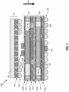
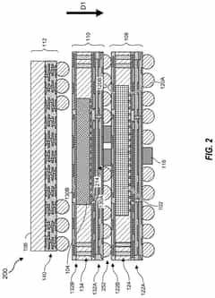
3D chiplet integration using fan-out wafer-level packaging
PatentPendingUS20240274587A1
Innovation
- The use of fan-out wafer-level packaging and three-dimensional packaging techniques for combining semiconductor chips and embedded memory in configurations such as face-to-back, back-to-back, and face-to-face orientations, enabling direct connections between chiplets and reducing assembly package sizes and manufacturing complexity.
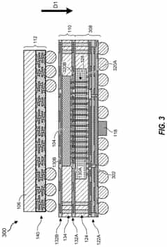
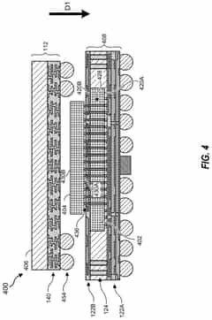
Integrated structure and integration method suitable for wafer-scale heterogeneous chiplet
PatentWO2024011880A1
Innovation
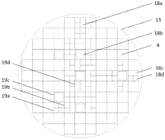
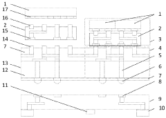
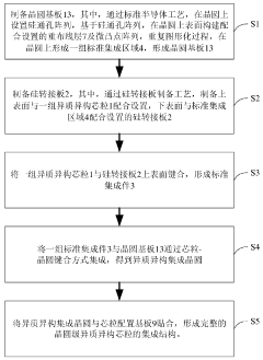
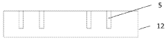
- By setting a through silicon via array and repeated standard integration areas on the wafer substrate, and preparing a silicon transfer board with heterogeneous transfer board micro-bumps and micro-pads, a standard integrated part is formed to realize heterogeneous cores. The die is bonded to the wafer substrate, and multi-layer rewiring layers are used to realize the interconnection between the die.
Intellectual Property Landscape
The intellectual property landscape surrounding chiplet technology has evolved rapidly in recent years, reflecting the growing strategic importance of this approach in semiconductor design. Major semiconductor companies including Intel, AMD, TSMC, and Samsung have been aggressively filing patents related to chiplet integration technologies, creating a complex web of intellectual property rights that new market entrants must carefully navigate.
Patent activity analysis reveals several key trends in chiplet technology. The most heavily protected areas include die-to-die interconnect technologies, packaging methods for heterogeneous integration, thermal management solutions, and testing methodologies for multi-die systems. Intel leads in overall patent count, with significant portfolios focusing on EMIB (Embedded Multi-die Interconnect Bridge) and Foveros technologies, while AMD has concentrated its efforts on securing IP around their Infinity Fabric interconnect.
Geographically, the United States and Taiwan dominate the patent landscape, though China has shown the fastest growth rate in chiplet-related patent filings over the past five years. This regional distribution closely mirrors the global semiconductor manufacturing ecosystem, with IP concentration following manufacturing capabilities.
The licensing landscape has also evolved significantly, with several industry consortia forming to address IP challenges. The Universal Chiplet Interconnect Express (UCIe) consortium represents a notable development, with founding members agreeing to license certain interconnect technologies under RAND (Reasonable and Non-Discriminatory) terms to promote industry standardization.
Patent litigation in the chiplet space remains relatively limited compared to other semiconductor technologies, suggesting that companies are currently focused on building their portfolios rather than engaging in aggressive enforcement. However, as the technology matures and market competition intensifies, increased litigation activity is anticipated, particularly around fundamental interconnect and packaging technologies.
Open-source initiatives are beginning to emerge as counterpoints to proprietary approaches, with organizations like CHIPS Alliance and RISC-V International promoting open specifications for chiplet interfaces. These efforts aim to reduce IP barriers to entry, though their impact remains limited compared to proprietary solutions backed by major industry players.
For companies entering the chiplet space, freedom-to-operate analyses have become increasingly complex, requiring careful navigation of overlapping patent claims across multiple technology domains including packaging, interconnect, power delivery, and system architecture.
Standardization Efforts in Chiplet Technology
The standardization of chiplet interfaces and protocols represents a critical foundation for the broader adoption and evolution of chiplet technology across the semiconductor industry. Several industry consortia and standards organizations have emerged to address the fragmentation challenges in chiplet integration methodologies.
The Universal Chiplet Interconnect Express (UCIe) consortium, formed in 2022, has rapidly established itself as a leading standardization effort. UCIe focuses on creating open die-to-die interconnect standards that enable chiplets from different vendors to communicate seamlessly. The standard defines both physical layer specifications and protocol stack implementations, covering aspects from electrical signaling to transaction protocols.
Complementing UCIe, the Open Compute Project (OCP) has developed the Bunch of Wires (BoW) specification, which provides a simpler, lower-cost alternative for chiplet interconnection. BoW emphasizes accessibility and ease of implementation, making it particularly suitable for applications where ultimate performance is less critical than cost-effectiveness.
JEDEC, a well-established semiconductor engineering standardization organization, has also entered the chiplet standardization space with its own working groups focused on memory integration with logic chiplets. Their efforts primarily address the specialized requirements of memory-intensive applications and high-bandwidth interfaces between memory and compute chiplets.
The Compute Express Link (CXL) Consortium, while not exclusively focused on chiplets, has developed standards that are increasingly relevant to chiplet integration, particularly for coherent memory access across different chiplets. CXL's cache coherency protocols provide essential functionality for complex multi-chiplet systems.
Patent analysis reveals that standardization efforts are creating new intellectual property landscapes. Companies are increasingly filing patents that build upon or extend these emerging standards, creating strategic positions around implementation methodologies and enhancement technologies.
The geographical distribution of standardization participation shows interesting patterns, with North American and East Asian companies dominating leadership positions in most consortia. European entities have focused more on specialized application domains and integration methodologies for automotive and industrial applications.
Looking forward, the convergence of these various standardization efforts will likely determine the trajectory of chiplet technology adoption. The industry appears to be moving toward a layered approach to standardization, with physical interconnects becoming increasingly standardized while leaving room for innovation in protocol implementations and system architecture.
Unlock deeper insights with PatSnap Eureka Quick Research — get a full tech report to explore trends and direct your research. Try now!
Generate Your Research Report Instantly with AI Agent
Supercharge your innovation with PatSnap Eureka AI Agent Platform!